SEARCH
検索詳細
喜多 隆学長・役員等理事
研究者基本情報
■ 学位■ 研究ニュース
- 2021年01月04日, 日常生活を取り戻す ウイルスフリー空調システムを開発
- 2018年04月13日, 神戸大学の教員3名が「科研費NEWS」に掲載されました
- 2017年04月07日, 変換効率50%を超えることができる新型太陽電池構造を提案―発電コストの大幅引き下げに期待―
- 2015年10月16日, 喜多隆教授が公益社団法人応用物理学会フェローの称号を授与されました
- 2015年05月15日, 水銀を使わないフィルム型紫外光源を世界で初めて開発
■ 研究分野
■ 委員歴
- 2022年04月 - 現在, 日本材料学会, 半導体エレクトロニクス部門委員会委員長
- 2006年04月 - 現在, 光物性研究会, 組織委員
- 1985年05月 - 現在, 応用物理学会, 正会員
- 2021年02月 - 2022年01月, レーザー学会年次大会, プログラム委員主査
- 1986年10月 - 2021年12月, 日本物理学会, 正会員
- 2021年04月 - 2021年10月, 9th International Symposium on Control of Semiconductor Interfaces (ISCSI IX, 2022), 国際プログラム委員
- 2019年10月 - 2021年10月, 電子材料シンポジウム(EMS), 実行委員長
- 2021年06月 - 2021年08月, SemiconNano 2021 (8th International Workshop on Epitaxial Growth and Fundamental Properties of Semiconductor Nanostructures), 組織委員長(共同)
- 2018年04月 - 2019年09月, 電子材料シンポジウム(EMS), 実行副委員長
- 2017年09月 - 2019年09月, 7th International Workshop on Epitaxial Growth and Fundamental Properties of Semiconductor Nanostructures (SemiconNano2019), 組織委員長
- 2018年02月 - 2019年05月, 2019化合物半導体ウィーク(CSW:ISCS&IPRM), 現地実行委員長
- 2018年09月 - 2019年04月, International Conference on Nanophotonics and Nano-optoelectronics, 組織委員会委員
- 2017年06月 - 2019年03月, 日本材料学会第66期編集委員会, 査読委員
- 2018年02月 - 2018年07月, 9th International Workshop on Bismuth-Containing Semiconductors, プログラム委員
- 2017年04月 - 2018年03月, レーザー学会学術講演会第38回年次大会, プログラム委員
- 2014年12月 - 2017年12月, 光物性研究会, 組織委員長
- 2017年06月 - 2017年10月, 国際シンポジウム (電気通信大学100周年記念)「“Future Earth”エネルギー課題に資する新奇なナノ物質・触媒・表面」, 組織委員
- 2016年04月 - 2017年08月, International Conference on Defects in Semiconductors(ICDS2017), International Program Committeeメンバー
- 2016年08月 - 2017年04月, International Conference on Nanophotonics and Nano-optoelectronics, 組織委員
- 2015年04月 - 2016年09月, 半導体レーザ国際会議(ISLC), 現地実行委員
- 2015年03月 - 2016年06月, 2016化合物半導体ウィーク(CSW:ISCS&IPRM), 展示委員長
- 2015年09月 - 2016年03月, 第17回ナノ構造における光と物質の相互作用に関する国際会議(PLMCN), 実行委員長
- 2015年01月 - 2015年09月, 2015年国際固体素子・材料コンファレンス, 論文副委員長
- 2013年07月 - 2015年07月, 電子材料シンポジウム(EMS), 論文委員長
- 2013年04月 - 2015年03月, 社団法人応用物理学会, 諮問委員
- 2002年04月 - 2013年06月, 電子材料シンポジウム, プログラム委員
- 2012年10月 - 2013年05月, 2013年化合物半導体週間(化合物半導体国際シンポジウム・インジウムリン系材料国際会議合同国際会議), 現地実行委員長
- 2011年04月 - 2013年03月, 社団法人応用物理学会, 理事
- 2009年07月 - 2012年09月, 第17回分子線エピタキシー国際会議, 現地実行委員長
- 2011年04月 - 2012年03月, Journal of Spectroscopy and Dynamics, Editorial Board
- 2009年03月 - 2011年08月, 第24回アモルファス及びナノ結晶半導体国際会議, 実行委員
- 2009年03月 - 2010年06月, 第37回化合物半導体国際会議, 論文委員(サブコミッティチェア)
- 2008年08月 - 2009年07月, EP2DS-18(第18回2次元電子系国際会議)/MSS-14(第14回半導体超構造国際会議), 現地実行委員長
- 2004年04月 - 2009年03月, Japanese Journal of Applied Physics, 編集委員
- 2006年11月 - 2007年10月, 第34回化合物半導体国際会議, 論文委員サブコミッティ幹事
- 2005年07月 - 2005年07月, 第14回分子線エピタキシー国際会議, 論文委員
- 2005年04月 - 2005年04月, 第18回インジウム燐および関連材料に関する国際会議, 組織委員
- 2003年04月 - 2005年03月, 応用物理学会, 関西支部幹事
- 2003年04月 - 2005年03月, 応用物理学会関西支部セミナー「光物性とその応用」, 世話人
- 1998年03月 - 2002年03月, 応用物理学会, 講演分科会世話人
- 1999年09月 - 2001年05月, 第13回インジウム燐および関連材料に関する国際会議, 組織委員
- 1995年04月 - 2000年03月, 日本光学会, 文献抄録委員
- 1993年05月 - 1998年03月, Spring-8利用者懇談会, 正会員
- 1993年07月 - 1996年12月, 日本真空協会, 個人会員
- 1992年07月 - 1996年12月, 日本金属学会, 正会員
- 1992年04月 - 1994年03月, 日本真空協会, 関西支部幹事
- 1992年03月 - 1993年08月, 第5回半導体不純物の物理と制御に関する国際会議, 組織委員
研究活動情報
■ 受賞- 2022年09月 9th International Symposium on Control of Semiconductor Interfaces (ISCSI-XI), ISCSI-XI Young Researcher Award, Photoluminescence Characteristics of InAs Quantum Dots in the Doubled-heterointerface of AlGaAs/GaAs-based Two-step Photon Up-conversion Solar Cells
- 2020年06月 47TH IEEE PHOTOVOLTAIC SPECIALISTS CONFERENCE (PVSC 47), PVSC 47 Best Student Paper Award, Up-converted photocurrent enhancement in modulation-doped two-step photon up-conversion
- 2020年03月 日本材料学会, 令和元年度日本材料学会論文賞, デュアルヘテロダイン干渉計により光源起因のノイズを低減したサブナノメートル精度ウエハフラットネス計測システム
- 2019年10月 電子材料シンポジウム, EMS賞, Efficient Laser Cooling in Rare-Earth Doped Oxides at High Temperature
- 2019年09月 SemiconNano, SemiconNano2019 Best Poster Award, Laser Cooling Utilizing Anti-Stokes Photoluminescence in Yb-Doped Yttrium Aluminum Garnet
- 2018年07月 日本材料学会半導体エレクトロニクス部門委員会, 日本材料学会半導体エレクトロニクス部門委員会平成30年度第1回研究会 学生優秀講演賞, Yb添加Yttrium-Aluminum化合物による固体レーザー冷却
- 2017年07月 日本材料学会半導体エレクトロニクス部門委員会, 日本材料学会半導体エレクトロニクス部門委員会 平成29年度第1回研究会 学生優秀講演賞, 低温キャップInAs/GaAs量子ドット超格子中間バンド型太陽電池における2段階光吸収の増強
- 2015年09月 応用物理学会, 応用物理学会フェロー表彰 第9回(2015年度), 半導体ナノ電子材料の構造制御と電子状態・光物性に関する研究
- 2014年12月 第25回光物性研究会, 光物性研究会奨励賞, InAs/GaAs量子ドット超格子太陽電池における高効率2段階光吸収過程
- 2014年11月 日本材料学会半導体エレクトロニクス部門委員会, 日本材料学会半導体エレクトロニクス部門委員会 平成24年度第3回研究会 学生優秀講演賞, 低次元量子構造を利用したホットキャリア型太陽電池の提案
- 2014年09月 応用物理学会, APEX/JJAP編集貢献賞, 2014年度(第13回)
- 2014年07月 平成26年度第2回半導体エレクトロニクス部門委員会第1回研究会, 日本材料学会半導体エレクトロニクス部門委員会平成26年度第1回研究会学生優秀講演賞, Dot-in-Well構造を用いた量子ドット太陽電池の室温二段階光吸収
- 2014年06月 40th IEEE Photovoltaic Special Conference, PVSC40 Best Student Paper Award, Carrier Time-of-Flight Measurement Using a Probe Structure for DirectEvaluation of Carrier Transport in Quantum Structure Solar Cells
- 2014年03月 第36回(2014年春季)応用物理学会, 応用物理学会講演奨励賞, プローブ構造を用いた量子構造太陽電池におけるキャリア走行時間の測定” トープラサートポン カシディット
- 2011年12月 The 18th International Display Workshops, IDW'11 Outstanding Poster Paper Award, Effects of Argon Plasma Irradiation on Amorphous In-Ga-Zu-Ofilm Evaluated by Microwave Photoconductivity Decay Method
- 2010年12月 第21回光物性研究会, 第21回光物性研究会奨励賞, 希土類化合物半導体GdNにおけるバンド端光吸収の磁気光学特性
- 2010年10月 6th International Workshop on Nano-Scale Spectroscopy \Nanotechnology, NSS6 Student Award, Band-Edge Structure Induced by Ferromagnetic Spin Ordering in GdN Thin Films
- 2009年12月 日本材料学会半導体エレクトロニクス部門委員会, 日本材料学会半導体エレクトロニクス部門学生優秀講演賞, 希土類窒化物半導体GdNヘテロ構造の基礎物性
- 2009年03月 財団法人エレクトロニクス実装学会, 第22回エレクトロニクス実装学会学術講演会優秀講演賞, 周期加熱サーモリフレクタンス法による銅めっき膜の熱伝導率評価
- 2008年12月 8th International Conference on Nano-Molecular Electronics 2008, ICNME2008 Outstanding Poster Presentation Award, Side Electron Emission Device Using A Composite of Carbon Nanofibers and Aluminum
- 2008年07月 ICOOPMA組織委員会, Best Poster Award, Lengthening of photoluminescence decay time owing to expansion of electron envelope functions in stacked quantum dots
- 2008年04月 電気関係学会関西支部連合大会実行委員会, 平成19年電気関係学会関西支部連合大会奨励賞, コラムナ量子ドットによる広帯域発光特性制御
- 2007年09月 応用物理学会, 応用物理学会講演奨励賞, InAs/GaAs量子ドット自己形成過程のRHEEDシェブロン構造のその場解析とIn拡散効果
- 2007年03月 日本金属学会, 金属学会写真奨励賞, 単一量子ドットの三次元微細構造解析
- 2006年11月 第67回応用物理学会学術講演会, 応用物理学会講演奨励賞, 高分解能断面TEMによる埋め込み量子ドット形状のマルチアングル直接観測
- 2005年05月 神戸大学, 神戸大学工学部優秀教育賞
- 2004年11月 はりま産学交流会主催, シーズコンペ入賞, 超省電力次世代ディスプレイ材料の開発
- 2000年09月 第46回応用物理学関係連合講演会, 応用物理学会講演奨励賞, Ga0.5In0.5P/GaAsヘテロ界面における自然超格子の影響 - 偏光ラマンスペクトル -
- 1999年09月 第60回応用物理学会学術講演会, 応用物理学会講演奨励賞, 反射率差分光法によるInAs自己形成量子ドット成長表面の観察
- 1998年07月 電子材料シンポジウム運営委員会, EMS賞, Time-Resolved Up-Converted Photoluminescence at Semicoductor Heterointerface
- 1995年07月 The Material Research Society of Japan, 日本MRS若手研究者アワード, AlGaInP混晶半導体自然超格子の電子状態制御
- Abstract The application of the thermoradiative effect of photodiodes, in which photons are emitted to a cold reservoir in the far-field, is a promising approach for renewable electricity generation. Here we derive the radiative limit of the output power density of an ideal thermoradiative diode (TRD) with an intermediate band (IB) using detailed balance calculations. The output power density of an ideal IB-TRD with a given bandgap energy and an optimal IB position increases with the device temperature, and simultaneously the optimal position of the IB shifts away from the mid-gap position due to the current matching constraint. Since the intrinsic carrier density needs to be significantly lower than the doping concentration to form a p–n junction at the operating temperature, IB-TRDs can be advantageous compared to single-junction TRDs consisting of narrow-bandgap semiconductors.Springer Science and Business Media LLC, 2025年03月, Scientific Reports, 15(1) (1)研究論文(学術雑誌)
- Abstract While a significant part of the solar energy lies in the infrared range, common semiconductors cannot absorb this part of the solar irradiance by direct band-to-band transitions, because the corresponding photon energies are below the bandgap energy. Two-step photon up-conversion (TPU) is one of the processes that allows us to harvest energy in the region below the bandgap, and one possible approach to realize a TPU-based solar cell is to use an AlGaAs/GaAs heterointerface with quantum dots in order to induce additional intraband transitions. On the other hand, here we report on the TPU phenomenon at a methylammonium lead bromide/gallium arsenide (MAPbBr3/GaAs) heterointerface without quantum dots. For this heterojunction, we observed high-energy photoemission by low-energy photoinjection, demonstrating the TPU. By using photoluminescence (PL) and time-resolved PL measurement techniques, we elucidate the mechanism of the PL emission from MAPbBr3 observed from MAPbBr3/GaAs samples. Through the comparisons of the experimental PL and TRPL results between the MAPbBr3/GaAs and MAPbBr3/Glass-substrate samples, we successfully distinguish the TPU phenomenon from the ordinal two-photon absorption of MAPbBr3. Our findings in the TPU at the MAPbBr3/GaAs heterointerface may help to realize quantum-dot-free photon up-conversion solar cells.Springer Science and Business Media LLC, 2025年01月, Journal of Optics, 英語[査読有り]研究論文(学術雑誌)
- Abstract We studied the photovoltaic properties of a conventional silicon photodiode under monochromatic illumination conditions to clarify the loss mechanisms that are important for application as a laser power converter. While the short-circuit current increases linearly with the excitation power, the power dependence of the open-circuit voltage consists of two regions with different slopes as a result of the Joule heating. At higher excitation power densities, thermal effects play a key role in the current–voltage characteristics, and therefore the maximum conversion efficiency is achieved at a certain excitation-power density. Furthermore, the optimum excitation wavelength shifts towards longer wavelengths as the excitation power density increases, because the optimum value is determined by a trade-off between the optical absorption strength and the excitation power density.IOP Publishing, 2025年01月, Japanese Journal of Applied Physics, 64(1) (1), 014001 - 014001, 英語[査読有り]研究論文(学術雑誌)
- American Chemical Society (ACS), 2024年12月, ACS Photonics, 12(1) (1), 447 - 456研究論文(学術雑誌)
- Abstract Two-step photon upconversion solar cells (TPU-SCs) based on III–V semiconductors can achieve enhanced sub-bandgap photon absorption because of intraband transitions at the heterointerface. From a technological aspect, the question arose whether similar intraband transitions can be realized by using perovskite/III–V semiconductor heterointerfaces. In this article, we demonstrate a TPU-SC based on a CsPbBr3/GaAs heterointerface. Such a solar cell can ideally achieve an energy conversion efficiency of 48.5% under 1-sun illumination. This is 2.1% higher than the theoretical efficiency of an Al0.3Ga0.7As/GaAs-based TPU-SC. Experimental results of the CsPbBr3/GaAs-based TPU-SC show that both the short-circuit current JSC and the open-circuit voltage VOC increase with additional illumination of sub-bandgap photons. We analyze the excitation power dependence of JSC for different excitation conditions to discuss the mechanisms behind the enhancement. In addition, the observed voltage-boost clarifies that the JSC enhancement is caused by an adiabatic optical process at the CsPbBr3/GaAs heterointerface, where sub-bandgap photons efficiently pump the electrons accumulated at the heterointerface to the conduction band of CsPbBr3. Besides the exceptional optoelectronic properties of CsPbBr3 and GaAs, the availability of a CsPbBr3/GaAs heterointerface for two-step photon upconversion paves the way for the development of high-efficiency perovskite/III–V semiconductor-based single-junction solar cells.Springer Science and Business Media LLC, 2024年11月, Scientific Reports, 14(1) (1)[査読有り]研究論文(学術雑誌)
- Abstract We report lateral photoconductive properties of multilayer-stacked undoped InAs/GaAs quantum dots (QDs) for the application of photoconductive terahertz (THz) antenna devices that operate in a 1.5 μm-telecom-wavelength band. The excitation power-dependent photocurrent showed a high value without saturation under high excitation power for the excitation wavelength of 1460 nm. From the reflection pump-probe signal, a fast photocarrier lifetime was derived. These results, together with the low dark current characteristic, support the applicability of the multilayer-stacked undoped InAs/GaAs QDs to photoconductive THz antennas operating in a 1.5 μm-wavelength band.IOP Publishing, 2024年08月, Japanese Journal of Applied Physics, 63(8) (8), 082002 - 082002研究論文(学術雑誌)
- Society of Materials Science, Japan, 2024年02月, Journal of the Society of Materials Science, Japan, 73(2) (2), 178 - 182, 日本語[査読有り]研究論文(学術雑誌)
- 公益社団法人応用物理学会, 2023年09月, 応用物理, 92(9) (9), 550 - 554, 日本語[査読有り]
- Abstract Ultrafast responses caused by ultrashort pulse excitation can be applied to ultrafast optical switches with high-speed information processing. In this paper, via the impulsive interference of excitons, we achieve an ultrafast optical response suited for ultrafast switches in all-optical networks. Due to the simultaneous excitation of two exciton states in the multiple quantum well on a strained buffer layer without the occurrence of adverse effects like stacking faults, impulsive interference is induced. The small compressive strain from the buffer layer modifies the orientation of the excitons inside the quantum well, and causes the ultrafast response.IOP Publishing, 2023年06月, Applied Physics Express, 16(6) (6), 062009 - 062009, 英語研究論文(学術雑誌)
- Photon upconversion (PU) is a process where an electron is excited from the valence band to the conduction band of a wide-gap semiconductor by the sequential absorption of two or more photons via real states. For example, two-step PU can generate additional photocurrent in the so-called intermediate-band solar cells. In this work, we consider two- and three-step processes; we study multi-step PU in a quantum dot (QD)-based single-junction solar cell with a double-heterointerface structure. The solar cell consists of three different absorber layers: Al0.7Ga0.3As, Al0.3Ga0.7As, and GaAs, which form two heterointerfaces. Just beneath each heterointerface, an InAs/GaAs QD layer was inserted. After band-to-band excitation, electrons accumulate at each heterointerface, and then, below-bandgap photons excite a certain fraction of these electrons above the barrier energy. The photoluminescence spectra of the InAs QDs reveal slightly different QD size distributions at the two heterointerfaces. We show that the external quantum efficiency is improved by additional irradiation with below-bandgap infrared photons, which suggests a multi-step PU process that involves the two heterointerfaces. The dependence of the photocurrent on the infrared excitation power density only shows a superlinear behavior when the GaAs layer is excited but the Al0.3Ga0.7As layer is not. These data demonstrate a multi-step PU process that consists of one intraband transition at each of the two heterointerfaces and one interband transition in GaAs.AIP Publishing, 2023年03月, Journal of Applied Physics, 133(12) (12), 124503 - 124503, 英語[査読有り]研究論文(学術雑誌)
- Abstract We elucidate a photocarrier collection mechanism in intermediate band solar cells (IBSCs) with InAs-quantum dots (QDs)-in-an-Al0.3Ga0.7As/GaAs-quantum well structures. When the Al0.3Ga0.7As barrier is excited, the device electrical output can be varied by additional infrared light for the electron intraband optical transition in QDs. The photocurrent in IBSC with a single QDs-in-a-well structure shows a monotonic increase with the intraband-excitation density. Conversely, IBSC with a multilayered QDs-in-a-well structure exhibits a photocurrent reduction when electrons in QDs are optically pumped out. The simultaneously measured photoluminescence spectra proved that the polarity of QD states changes depending on the intraband-excitation density. We discuss the drift and diffusion current components and point out that the hole diffusion current is significantly influenced by carriers inside the confinement structure. Under strong intraband excitations, we consider an increased hole diffusion current occurs by blocking hole-capture in the quantum structures. This causes unexpected photocurrent reduction in the multilayered device.IOP Publishing, 2022年07月, Japanese Journal of Applied Physics, 61(7) (7), 074002 - 074002[査読有り]研究論文(学術雑誌)
- Optica Publishing Group, 2022年03月, Optics Express, 30(7) (7), 11789 - 11789, 英語[査読有り]研究論文(学術雑誌)
- AIP Publishing, 2022年02月, AIP Advances, 12(2) (2), 025110 - 025110[査読有り]研究論文(学術雑誌)
- 2022年01月, Chemistry&Chemical Industry(化学と工業), 75(1) (1), 26 - 28, 日本語紫外光によるウイルスの不活化と実証実験[招待有り]研究論文(学術雑誌)
- This article was originally published online on 29 September 2021 with author Takashi Kita incorrectly spelled. The name is correct as it appears above. All online versions of this article were corrected on 5 October 2021 the article is correct as it appears in the printed version of the journal. AIP Publishing apologizes for this error.American Institute of Physics Inc., 2021年11月, Journal of Applied Physics, 130(17) (17), 英語研究論文(学術雑誌)
- AIP Publishing, 2021年09月, Journal of Applied Physics, 130(12) (12), 124505 - 124505[査読有り]研究論文(学術雑誌)
- AIP Publishing, 2021年08月, Journal of Applied Physics, 130(8) (8), 085701 - 085701, 英語[査読有り]研究論文(学術雑誌)
- IOP Publishing, 2021年08月, Journal of Physics D: Applied Physics, 54(33) (33), 335106 - 335106[査読有り]研究論文(学術雑誌)
- The Optical Society, 2021年07月, Optics Express, 29(15) (15), 24387 - 24387[査読有り]研究論文(学術雑誌)
- Nanostructured intermediate band solar cells have been proposed as one of the promising candidates to surpass the limited efficiency of single-junction photovoltaic devices, while challenges still remain for realizing their practical implementation due to intricate carrier behaviors occurring in confined states. In this report, we have elucidated a detailed photo-carrier collection mechanisms in a quantum dot-in-well intermediate band solar cell, which is varied by effective electron intraband excitation process. Results from the photoluminescence response of quantum dots are discussed to examine the occupation state inside confined levels. Detailed analyses point out that diffusion of holes plays an important role in modulating the electrical generations.Institute of Electrical and Electronics Engineers Inc., 2021年06月, Conference Record of the IEEE Photovoltaic Specialists Conference, 1786 - 1788, 英語研究論文(国際会議プロシーディングス)
- 2021年05月, KOGAKU Japanese Journal of Optics, 50(10) (10), 432 - 437解説:希土類イオンを利用した水銀フリ-ナロ-バンド紫外光源[査読有り]
- SPIE, 2021年04月, Photonic Heat Engines: Science and Applications III[査読有り]研究論文(国際会議プロシーディングス)
- APL Editor's PicksAIP Publishing, 2021年02月, Journal of Applied Physics, 129(7) (7), 074503 - 074503, 英語[査読有り]研究論文(学術雑誌)
- Society of Materials Science, Japan, 2020年10月, 材料, 69(10) (10), 727 - 732, 日本語[査読有り]研究論文(学術雑誌)
- {AIP} Publishing, 2020年09月, AIP Advances, 10(9) (9), 095016 - 095016, 英語[査読有り]研究論文(学術雑誌)
- IOP Publishing, 2020年08月, Japanese Journal of Applied Physics, 59(8) (8), 082005 - 082005, 英語[査読有り]研究論文(学術雑誌)
- American Physical Society (APS), 2020年07月, Physical Review Applied, 14(1) (1), 014010-1 - -7, 英語[査読有り]研究論文(学術雑誌)
- 2020年07月, Applied Physics Letters, 117(041104) (041104), 1 - 5, 英語[査読有り]研究論文(学術雑誌)
- Springer Science and Business Media LLC, 2020年07月, Scientific Reports, 10(1) (1)[査読有り]研究論文(学術雑誌)
- Intermediate-band solar cell is one of the promising concepts to jump out the dilemma of limited efficiency for traditional single junction photovoltaic devices. Albeit fruitful explorations have been done on revealing its working principle and promoting output performance, optical and electrical match of outer system can sometimes get it complicated because of extra below-bandgap photon absorptions. In this study, we reported a voltage backtracking behavior under intensive bi/uni-color irradiation circumstance within this kind of cell. Two different mechanisms are separately disclosed here for the sake of deep understanding how it operates and by which it can better work.Institute of Electrical and Electronics Engineers Inc., 2020年06月, Conference Record of the IEEE Photovoltaic Specialists Conference, 2020-, 0146 - 0148, 英語研究論文(国際会議プロシーディングス)
- Two-step photon up-conversion solar cell is a newly-proposed concept for high-conversion efficiency photovoltaics, in which a heterointerface of different semiconductor materials is delicately merged inside common single-junction cell structure. Recently, we have reported an enhancement of its photocurrent under a reverse bias condition due to the boosted carrier collection efficiency. To push it further, in this study, modulation-doping method is employed in order for a better elucidation of two-step photon up-conversion at the heterointerface. It is observed that the difference of the external quantum efficiency with additional infrared light irradiation on the TPU-SCs can be greatly enlarged by changing doping concentration selectively reflecting the importance of the electric field at the heterointerface.Institute of Electrical and Electronics Engineers Inc., 2020年06月, Conference Record of the IEEE Photovoltaic Specialists Conference, 2020-, 0902 - 0904, 英語研究論文(国際会議プロシーディングス)
- AIP Publishing, 2020年06月, Review of Scientific Instruments, 91(6) (6), 065114 - 065114, 英語[査読有り]研究論文(学術雑誌)
- SPIE, 2020年02月, Photonic Heat Engines: Science and Applications II, 11298, 112980B-1 - 10, 英語[査読有り]研究論文(国際会議プロシーディングス)
- 2020年02月, Jpn. J. Appl. Phys., 59, 032002-1 - 5, 英語[査読有り]研究論文(学術雑誌)
- IOP Publishing, 2019年12月, Applied Physics Express, 12(12) (12), 125008 - 125008, 英語[査読有り]研究論文(学術雑誌)
- The Optical Society, 2019年11月, Optics Express, 27(24) (24), 34961 - 34961, 英語[査読有り]研究論文(学術雑誌)
- Society of Materials Science, Japan, 2019年10月, Journal of the Society of Materials Science, Japan, 68(10) (10), 762 - 766[査読有り]研究論文(学術雑誌)
- 2019年10月, 材料 別冊, 68(10) (10), 762 - 766, 日本語Yb添加イットリウムアルミニウムガーネット結晶粉末におけるアンチストークス発光を利用した理想レーザー冷却効率[査読有り]研究論文(学術雑誌)
- 2019年10月, 材料 別冊, 68(10) (10), 757 - 761, 日本語金属上に形成した2次元フォトニック結晶の光学応答[査読有り]研究論文(学術雑誌)
- 2019年10月, 材料 別冊, 68(10) (10), 767 - 771, 日本語加速度計により振動の影響を低減したサブナノメートル精度ウエハフラットネス計測システム[査読有り]研究論文(学術雑誌)
- American Chemical Society (ACS), 2019年08月, J. Phys. Chem, 123(32) (32), 19447 - 19452[査読有り]研究論文(学術雑誌)
- IOP Publishing, 2019年08月, Semiconductor Science and Technology, 34(9) (9), 094003 - 1-5, 英語[査読有り]研究論文(学術雑誌)
- AIP Publishing, 2019年07月, Journal of Applied Physics, 126, 033103 - 1-6, 英語[査読有り]研究論文(学術雑誌)
- We developed a method of growing closely stacked InAs/GaAs quantum dots (QDs) to control the photoluminescence (PL) polarization characteristics in a wide wavelength range. The emission wavelength of the closely stacked QDs redshifted with decreasing substrate temperature during stacking growth, while the PL polarization characteristic was controlled by the GaAs spacer layer thickness and the number of QD layers. A unified rule for the optimum GaAs spacer layer thickness that both enhances the transverse magnetic (TM)-polarized component and achieves a high PL intensity for all growth temperatures was revealed. 30-layer stacked QDs with the optimum spacer layer thickness grown at substrate temperatures from 430 to 480 °C exhibited TM-enhanced polarization characteristics in the 1.15-1.3 μm band. Moreover, we studied the one-dimensional electronic states in the closely stacked QDs with the optimized GaAs spacer layer thickness by time-resolved PL.American Institute of Physics Inc., 2019年06月, Journal of Applied Physics, 125(23) (23), 英語研究論文(学術雑誌)
- Two-step photon up-conversion solar cell (TPU-SC) we have recently proposed is a single-junction solar cell containing a hetero-interface of different semiconductor materials. Although efficient two-step photon up-conversion is achieved in the TPU-SC, the detailed mechanism of the significant intraband photoexcitation occurring at the hetero-interface is still unclear. In this study, we performed simultaneous measurements of photoluminescence and photocurrent as a function of the applying bias voltage in the TPU-SC. We experimentally demonstrate the reciprocity relationship between the radiative recombination and the photocurrent of the TPU-SC.Institute of Electrical and Electronics Engineers Inc., 2019年06月, Conference Record of the IEEE Photovoltaic Specialists Conference, 2623 - 2626, 英語研究論文(国際会議プロシーディングス)
- We have recently proposed a solar cell (SC) structure called two-step photon up-conversion SC (TPU-SC). In this SC, we have observed an obvious enhancement in the open- circuit voltage as well as the short-circuit current. In this study, we investigated the excitation intensity dependence of TPU. We find that the extra-photocurrent caused by TPU shows a sublinear relationship with the interband excitation intensity. In addition, the enhancement of the open-circuit voltage by TPU is larger than the value estimated from the short-circuit current, suggesting a voltage-boost at the hetero-interface.Institute of Electrical and Electronics Engineers Inc., 2019年06月, Conference Record of the IEEE Photovoltaic Specialists Conference, 2597 - 2599, 英語研究論文(国際会議プロシーディングス)
- We demonstrated hot-carrier (HC) extraction in GaAs solar cells containing InAs/GaAs quantum dot superlattices (QDSLs) functioning as a light absorber at 15 K. The short-circuit current density and the open-circuit voltage in the QDSL solar cells show step-wise changes as a function of the excitation photon density because of state filling under below-bandgap excitation. Furthermore, the short-circuit current density and the open-circuit voltage originated from the HC extraction were enhanced by increasing the period of the QDSL due to the improved absorptivity.Institute of Electrical and Electronics Engineers Inc., 2019年06月, Conference Record of the IEEE Photovoltaic Specialists Conference, 3004 - 3006, 英語研究論文(国際会議プロシーディングス)
- Institute of Physics, 2019年05月, Journal of Physics: Conference Series, 1220, 012013 - 1-4, 英語[査読有り]研究論文(国際会議プロシーディングス)
- We studied the dynamics of electrons generated by two-step photoexcitation in an intermediate-band solar cell (IBSC) comprising InAs/GaAs/Al0.3Ga0.7As dot-in-well (DWELL) structure using time-resolved photocurrent (TRPC) measurement. The examined IBSC exhibited considerably slower photocurrent decay than a conventional InAs/GaAs quantum dot IBSC, which is due to the extraordinaNature Publishing Group, 2019年05月, Scientific Reports, 9, 7859 - 1-8, 英語[査読有り]研究論文(学術雑誌)
- OSA Publishing, 2019年04月, OSA Continuum, 2, 1621 - 1628, 英語[査読有り]研究論文(学術雑誌)
- 2019年03月, Physica E: Low-dimensional Systems and Nanostructures, 111, 179 - 184, 英語[査読有り]研究論文(学術雑誌)
- Nature Publishing Group, 2019年02月, Nature Communications, 10, 956 - 1-3, 英語[査読有り]研究論文(学術雑誌)
- We developed a heterodyne interferometry system cancelling the noise caused by floor vibration and mechanical vibration using accelerometers. The interferometry is one of the powerful tools to precisely measure the flatness of a polished semiconductor wafer. Generally, the noise caused by vibration affects the displacement measured by the interferometers, and it is difficult to completely avoid the noise even if we use a vibration isolation table or perform motor tuning of the driving parts. The noise cancelling has been conducted by compensating the distance between a pair of interferometers using the signals obtained by accelerometers mounted on near the interferometers. Here, we propose and demonstrate a noise cancelling method. Utilizing the system, we successfully reduced the influence of floor vibration and mechanical vibration, and the precision of the measurement of the wafer flatness has been improved 38% by the technique in this experiment.Society of Materials Science Japan, 2019年, Zairyo/Journal of the Society of Materials Science, Japan, 68(10) (10), 767 - 771, 日本語研究論文(学術雑誌)
- In the previous chapter, we discussed the conditions that apply to the actual solar cell but were not considered for the ideal solar cell. In order to derive the maximum output power of the actual solar cell, we have to discuss the balance between absorption (resulting in electrical current) and emission (due to the established voltage). Therefore, the present chapter discusses the balanced condition of voltage and current by employing the current–voltage relation determined in the previous chapter. Based on that, the conversion efficiency of the actual solar cell is derived. Then, we discuss the contributions of the different types of losses that occur in a solar cell with a single band gap.Springer Verlag, 2019年, Green Energy and Technology, 55 - 79, 英語論文集(書籍)内論文
- In Chap. 5, we derived the single-junction solar cell conversion efficiency within the framework of the detailed balance theory and computed the solar spectrum by employing Planck’s law for black-body radiation. As explained in Sect. 2.2, the solar spectrum that passes the atmosphere differs according to the amount of air passed. This amount can be expressed as air mass (AM). In this chapter, we do not rely on the black-body radiation for the solar spectrum, but employ the actual spectral data for the sunlight that reaches the Earth after passing the atmosphere. With this data, we calculate the conversion efficiencies of several different solar cell structures. We first recalculate the conversion efficiency of the single-junction solar cell in Sect. 6.1 by using the real solar spectrum. In Sect. 6.2, we determine the conversion efficiency of a solar cell under concentrated sunlight, which can be obtained, for example, by using a lens. Additionally, in Sects. 6.3–6.6 we discuss four selected solar cell structures that are recently attracting attention as novel types of solar cells with the ability to overcome the S–Q limit. To exceed the S–Q limit means that the transmission and thermalization losses, which we declared as “being unavoidable,” have to “be avoided somehow” by using novel approaches. For the reduction of the losses and conversion of the sunlight into electrical power to the best extent possible, we can either increase the wavelength range that is employed by the solar cell for conversion into electrical power, or the opposite, and we can reshape the solar spectrum itself in such a way that it can be efficiently converted into electrical power by the solar cell. As examples for the first-mentioned approach, we discuss the multi-junction solar cell (which can also be called tandem solar cell) in Sect. 6.3 and the intermediate-band solar cell in Sect. 6.4. Multi-junction solar cells comprise a multilayer structure where each of the stacked layers is a semiconductor junction with different Eg. This method enables capturing the light transmitted through one solar cell by another solar cell in the layer below. Therefore, the light that would usually be lost through transmission can be used for electricity generation, and this allows us to exceed the S–Q limit of the single junction. This solar cell architecture has already been practically implemented, and the multi-junction type is the current world record holder in terms of solar cell performance. Unfortunately, the series connection between the junctions constitutes a drawback for the multi-junction solar cells. The tandem solar cells consist of stacked junctions that are serially connected. Therefore, the electricity generation is already completely suppressed if one of the stacked junctions does not operate. For example, a certain spectral part of the light may hardly reach the solar cell due to the scattering and absorption in clouds on a cloudy day. If due to this the electricity generation of any solar cell in the stack drops, the performance of the whole device is affected because the current that flows through the directly affected cell is reduced and becomes the bottleneck of the whole device, even if the solar cells in the other layers work fine. On the other hand, the intermediate-band solar cell has attracted attention as a solar cell architecture that promises high conversion efficiencies and can also lift the restrictions imposed by the series connection of the multi-junction tandem solar cells. This architecture reduces the transmission losses by implementing a new band (the so-called intermediate band) within the band gap of the solar cell. Because the direct absorption of the light via a transition between the conduction and the valence bands (a so-called interband transition) occurs in parallel with the stepwise absorption via the intermediate band, the intermediate-band solar cell’s electricity generation cannot be completely suppressed under clouded conditions as was the case for the multi-junction solar cells. In the intermediate-band solar cell, by absorbing a below-gap photon, an electron transits from the valence band to the intermediate band. Upon absorbing another below-gap photon, the electron is further excited into the conduction band. There transitions widely cover the solar spectrum. This two-step excitation (two-step photon up-conversion) process following the absorption of two below-gap photons produces additional photocurrent without degrading the photovoltage. Such two-step photoexcitation is known to occur at heterointerfaces. In Sect. 6.5, we deal with a solar cell containing a heterointerface in the intrinsic layer so-called two-step photon up-conversion solar cell. The conversion efficiency of the solar cell utilizing interband and intraband transitions strongly depends on the absorptivity of these transitions. Detailed influences of the absorptivity of photovoltaic materials on the conversion efficiency are also discussed. Section 6.6 discusses one example for the reduction of losses by altering the solar spectrum. To reduce the transmission losses, it is necessary to convert the light in the long-wavelength region of the solar spectrum into light with shorter wavelengths. Similarly, to reduce losses through thermalization, it is necessary to convert the light in the short-wavelength region of the solar spectrum into light with longer wavelengths. We analyze how much the conversion efficiency can be improved by down-converting the short-wavelength light (high photon energies) to long-wavelength light (small photon energies). Besides, the influences of changing weather conditions on the conversion efficiency of various types of solar cells are introduced in detail in Sect. 6.7. Up to Sect. 6.7, we proceed to discuss the solar cell at a constant temperature of 300 K. However, since concentration of sunlight is an important technique to enhance conversion efficiencies, the influence of the temperature has to be investigated. Due to the strong concentration of sunlight, the temperature of the concentrator solar cell device increases. If the temperature increases, the semiconductor band gap becomes smaller and furthermore, a higher the electron–hole recombination rate (stronger black-body radiation) is observed as explained in Sect. 4.2 this causes a decrease in the conversion efficiency. In Sect. 6.8, we analyze the change in the single-junction solar cell efficiency that occurs upon a change in the solar cell temperature. The solar cell is the photovoltaic device used as a solar energy converter. When indoor light such as white light-emitting diode (LED) is harvested, the optimized energy structure of the photovoltaic materials is different from the results obtained for the sunlight. We touch the energy conversion efficiency of indoor photovoltaic cells in Sect. 6.9.Springer Verlag, 2019年, Green Energy and Technology, 81 - 137, 英語論文集(書籍)内論文
- The solar cell is a device that converts the energy of light into electrical energy. Consequently, a prerequisite for the derivation of the conversion efficiency of a solar cell is to understand the nature of light energy. In the present chapter, we clarify what energy is contained in light and explain the characteristics of the light that is emitted from the sun.Springer Verlag, 2019年, Green Energy and Technology, 15 - 24, 英語論文集(書籍)内論文
- The solar cells that are discussed in this book are based on semiconductors. The degree of difficulty in the explanation of the properties of semiconductors greatly depends on the starting point of the explanations. In this book, we start with the fact that “a semiconductor is formed by a valence band which is completely filled with electrons and an empty conduction band, both bands being separated by a characteristic energy gap.” First, we shall investigate the behavior of the bands in the representative semiconductor silicon (Si) to clarify the band-gap concept. Then, we provide explanations on the intrinsic semiconductors which contain no impurities, and the extrinsic semiconductors wherein impurity atoms with a different number of valence electrons are added. Within the extrinsic semiconductors, we distinguish between the n-type semiconductor with excess electrons that are delivered to the conduction band and the p-type semiconductor with the so-called holes (i.e., missing electrons) that are delivered to the valence band. Regarding these two classes of semiconductors with different electronic conditions, we clarify the details about the density of electrons and holes, their distributions, and the so-called Fermi level (which is the energy level corresponding to an electron occupation probability of 50%). We also consider the transport of electrons and holes inside the semiconductor. Finally, we derive the characteristics of the p–n junction, which connects an n-type semiconductor with a p-type semiconductor and is commonly used for solar cell devices. The present chapter provides detailed explanations from the viewpoint of the semiconductor electronics, which makes it accessible with the knowledge equivalent to that of a third-year undergraduate student. With respect to the structure of the present book, not all details mentioned in this chapter are required for the understanding of the other chapters. In other words, the calculation of the energy conversion efficiency of a solar cell, which is the target of the present book, is based on a relatively independent approach. The reader may omit this chapter, or regard it as a guide to find concrete ideas for improving the conversion efficiencies of semiconductor solar cells. In order to enable an independent study of this chapter on semiconductors, we again define all variables of the previous chapters.Springer Verlag, 2019年, Green Energy and Technology, 157 - 202, 英語論文集(書籍)内論文
- The solar cells covered in the previous chapters are idealized solar cells, which allowed us to evaluate the efficiency limits under various conditions. Of course, besides the conditions employed so far (like the transmission of photons with Ephoton < Eg), there exist plenty of other factors that lead to losses in the amount of generated electricity and thus are important for the actual development of solar cells. Due to these losses, the conversion efficiency of an actually fabricated solar cell is smaller than the theoretical efficiency limit. For example, if we use silicon (Si) for the solar cell absorber material, the detailed balance limit of the conversion efficiency is about 30%. This value can be obtained from Fig. 5.10 in Chap. 5 by looking up the efficiency for the curve (b) at 1.1 eV, which is the band gap of Si. On the other hand, when we look up the present values for actual Si p–n junction solar cells, we find that the single crystal type has reached a maximum of 26.3% and the multi-crystalline type has reached a maximum of 22.3%, both being well below the theoretical efficiency limit[1]. In Chap. 3, we discussed the trade-off relation between the transmission and thermalization losses in the single-junction solar cell and derived the conversion efficiency limit that is imposed by these two types of losses. In considerations on the solar cell performance, such trade-off relations exist for various parameters. As another example for a trade-off relation, in the following sections, we introduce the semiconductor light absorption characteristics, which differ for each material. With this new concept, we discuss the solar cell conversion efficiency from a viewpoint that is different from the detailed balance model elaborated in the previous chapters. The trade-off presented in the following sections is a trade-off between the thickness of the semiconductor that is required for sufficient light absorption and the distance that can be travelled by the generated electrons and holes. The latter property is essential for the efficient extraction of carriers at the electrodes. It is straightforward that a thicker semiconductor can absorb more light. On the other hand, if the semiconductor is too thick, the distance that has to be travelled by the photoexcited electrons and holes also becomes longer. If the path to be travelled is long, there is a high probability for the electron to collide with an obstacle before its electrical energy can be used. Then the energy is unfortunately lost in spite of the efforts to generate it. A thicker semiconductor is not necessarily better we have to consider the optimum thickness for efficient extraction of the electrical energy. After discussing the light absorption characteristics of semiconductors in Sect. 7.1, we explain the transport of the generated electrons and holes inside the semiconductor in Sect. 7.2. In the last section, we consider two specific semiconductor materials, Si and GaAs, as examples and discuss the optimum semiconductor thickness in a solar cell.Springer Verlag, 2019年, Green Energy and Technology, 139 - 156, 英語論文集(書籍)内論文
- The goal of this book is to derive the conversion efficiency under consideration of the equilibrium between the carrier generation and recombination that occurs in the solar cell (i.e., under consideration of the detailed balance principle). As a step toward this goal, we shall first determine the most basic conversion efficiency. The ideal efficiency curve u(νg, Ts), which is derived in this chapter, is the basis of all conversion efficiency curves that are presented in the following chapters and thus constitutes an important relation. Besides the mathematical derivation of the ideal efficiency curve u(νg, Ts), the present chapter also explains a visual approach, that is, a graphical solution for the efficiency curve, which provides a deeper understanding of u(νg, Ts). With this visual approach, the reader can intuitively estimate the value of the ideal solar cell conversion efficiency without the need of solving the equations. In this chapter, we first provide the definition of the solar cell conversion efficiency, and then explain details about the efficiency losses induced by the semiconductor band gap, and finally, we derive the energy conversion efficiency of the ideal solar cell.Springer Verlag, 2019年, Green Energy and Technology, 25 - 42, 英語論文集(書籍)内論文
- In the previous chapter, we determined the ideal conversion efficiency u(νg, Ts) of an ideal solar cell. Since we wanted to know the limiting efficiency in the most ideal case, we neglected effects like internal generation of radiation and luminescence. However, the relation between the voltage and the current in an actual solar cell that employs a semiconductor diode (i.e., a p–n junction) is incompatible with the assumptions in Sect. 3.4 (these assumptions enabled us to set the electromotive force equal to that provided by the potential Eg/e). In the present chapter, we analyze the conversion efficiency of a solar cell that possesses a nonzero temperature. By including losses that arise due to the very fact of a finite solar cell temperature, the relation between the current and voltage is derived, and then, we determine the open-circuit voltage and the short-circuit current.Springer Verlag, 2019年, Green Energy and Technology, 43 - 54, 英語論文集(書籍)内論文
- We derive the conversion efficiencies of solar cells under various conditions in the chapters following Chap. 3. For our discussions on the solar cell conversion efficiency, it is extremely important to first understand the principle of electricity generation in a solar cell. In contrast to the electrochemical cell, which is usually introduced in high-school grade chemistry, the opportunities to study the operation principle of solar cells are almost zero except for some specialized schools. Most solar cells consist of a semiconductor p–n junction, which is a connection between a semiconductor n-layer with many electrons and a semiconductor p-layer containing plenty of holes in the semiconductor crystal. Even if high-school lectures on solar cells could be established, we have in mind that the explanation of how the electricity generation exactly works in such solar cells often will have to be skipped and summarized as “knowledge belonging to the category of semiconductor engineering.” On hearing the rather famous word semiconductor, one may think of realms of science completely different from the electrochemical cell. Since there are too many things that have to be learned regarding semiconductor materials, many of those who try studying the operation principle of solar cells may have difficulties to immediately grasp all essential relations.In this chapter, we explain how the solar cell converts the energy supplied by the Sun into electrical energy. For this, we employ the example of the well-known electrochemical cell, in particular, the “voltaic pile” which was most likely studied first in high school, and compare it with the solar cell from the viewpoint of the redox reactions. In order to easily grasp the idea of how current flows, the explanations especially emphasize the electron movement that occurs inside the solar cell.After explanation of the operation principle of the voltaic pile on a high-school chemistry level in Sect. 1.1, we explain the principle of electricity generation in a solar cell while outlining the parallels to the electrochemical cell. Finally, we clarify the unique qualities of the solar cell by discussing the similarities and differences between these types of “cells,” i.e., the electrochemical cell and the solar cell.Springer Verlag, 2019年, Green Energy and Technology, 1 - 13, 英語論文集(書籍)内論文
- Springer Singapore, 2019年, Green Energy and Technology[査読有り]
- Development of high-efficiency solar cells is one of the attractive challenges in renewable energy technologies. Photon up-conversion can reduce the transmission loss and is one of the promising concepts which improve conversion efficiency. Here we present an analysis of the conversion efficiency, which can be increased by up-conversion in a single-junction solar cell with a hetero-interface that boosts the output voltage. We confirm that an increase in the quasi-Fermi gap and substantial photocurrent generation result in a high conversion efficiency.Nature Publishing Group, 2018年12月, Scientific Reports, 8(1) (1), pp. 872 - 1-8, 英語[査読有り]研究論文(学術雑誌)
- Recently, we have proposed a new type solar cells utilizing photon up-conversion phenomenon, called two-step photon up-conversion solar cells for realizing high conversion efficiency solar cells. Here, achieving efficient intraband photoexcitation is indispensable. This solar cell has a simple single- j unction structure containing a hetero-interface. In this study, we investigated the applying electric field dependence of two-step photon up-conversion occurring at the hetero-interface. We found that dense electron accumulation and an appropriate electric field enable to dramatically increase the intraband excitation strength and the carrier collection efficiency at the hetero-interface.Institute of Electrical and Electronics Engineers Inc., 2018年11月, 2018 IEEE 7th World Conference on Photovoltaic Energy Conversion, WCPEC 2018 - A Joint Conference of 45th IEEE PVSC, 28th PVSEC and 34th EU PVSEC, 3447 - 3450, 英語研究論文(国際会議プロシーディングス)
- 2018年11月, Proceedings of the 35th European Photovoltaic Solar Energy Conference and Exhibition, 126 - 128, 英語[査読有り]研究論文(国際会議プロシーディングス)
- 2018年10月, Physical Review Applied, A 10(044035) (044035), pp. 044035 - 1-6, 英語[査読有り]研究論文(学術雑誌)
- We developed a heterodyne interferometry system cancelling the noise caused by a light source using a pair of heterodyne interferometers. The interferometry is one of the powerful tools to precisely measure the flatness of a polished semiconductor wafer. Generally, the noise caused by a light source affects the change of distance measured by interferometers, and it is difficult to avoid the noise by filtering a lock-in-amplification process. Here, we demonstrate that a pair configuration of interferometers synchronizing each other dramatically cancels the noises. The noise cancelling has been conducted by replacing the arrangement of the modulation frequency of two light waves producing an interference signal in one and the other interferometer each other. Utilizing these noise-cancelling heterodyne interferometers, we characterized the flatness of a polished silicon wafer. The precision has been improved 16% by the noise cancelling, and the system has enabled the measurement of the wafer flatness with repeatability of 0.32 nm.Society of Materials Science Japan, 2018年09月, Zairyo/Journal of the Society of Materials Science, Japan, 67(9) (9), 829 - 833, 日本語研究論文(学術雑誌)
- 2018年09月, 材料 別冊, Vol. 67(No. 9) (No. 9), pp. 829 - 833, 日本語デュアルヘテロダイン干渉計により光源起因のノイズを低減したサブナノメートル精度ウエハフラットネス計測システム[査読有り]研究論文(学術雑誌)
- 2018年07月, Applied Physics Express, Vol. 11(No. 1) (No. 1), pp.082303 - 1-4, 英語Hot-Carrier Generation in a Solar Cell Containing InAs/GaAs Quantum-Dot Superlattices as a Light Absorber[査読有り]研究論文(学術雑誌)
- Institute of Physics, 2018年07月, Journal of Physics D: Applied Physics, 51, 305102 - 1-6, 英語[査読有り]研究論文(学術雑誌)
- 2018年06月, 電気評論, (6月号) (6月号), 13 - 17, 日本語高変換効率太陽光発電の研究開発~50%を超える変換効率実現に向けた取り組み[査読有り]
- We present a Si-photonics-based quantum dot heterogeneous tunable lasers in the 1-μm band. Optical devices using Si-photonics-based PIC in the 1-μm band probably have not been reported yet.OSA - The Optical Society, 2018年, Optics InfoBase Conference Papers, 2018, 英語[査読有り]研究論文(国際会議プロシーディングス)
- We have proposed a two-step photon up-conversion solar cell (TPU-SC), which is a single junction solar cell comprising a wide gap semiconductor (WGS) and a narrow gap semiconductor (NGS) to break through the Shockley-Queisser limit for the single-junction solar cells. In the TPU-SC, below-gap photons of WGS excite the NGS and accumulate electrons at the WGS / NGS hetero-interface. The accumulated electrons at the hetero-interface are easily excited towards the WGS barrier by the low-energy photons, resulting in the efficient two-step up-conversion (TPU). We have experimentally demonstrated highly efficient current generation by the TPU. In this paper, we present the concept of the TPU-SC, theoretical prediction of the conversion efficiency of the TPU-SC, and experimental result of efficient photocarrier collection attributable to the TPU phenomenon.SPIE, 2018年, Proceedings of SPIE - The International Society for Optical Engineering, 10527, 英語[査読有り]研究論文(国際会議プロシーディングス)
- We studied intermediate-band solar cells (IBSCs) incorporating highly homogeneous InAs/GaAs quantum dot superlattices (QDSLs). The extra photocurrent generated by two-step photon absorption markedly increases at the fundamental state (FS) because the FS miniband has been successfully formed in the QDSL-IBSC by controlling the QD size homogeneity. Here, the carriers excited into the miniband spatially separate in the internal electric field, and the long-lived electrons in the intermediate states of the miniband increase the inter-subband absorption strength. The two-step photocurrent response, therefore, extends toward the longer-wavelength side corresponding to the QDSL-FS at approximately 1.2 mu m. (C) 2018 The Japan Society of Applied PhysicsIOP PUBLISHING LTD, 2018年01月, APPLIED PHYSICS EXPRESS, 11(1) (1), pp. 012301 - 1-4, 英語[査読有り]研究論文(学術雑誌)
- Small numbers of nitrogen dopants dramatically modify the electronic properties of GaAs, generating spatially localized resonant states within the conduction band, pair and cluster states in the band gap, and very large shifts in the conduction-band energies with nonlinear concentration dependence. Cross-sectional scanning tunneling microscopy provides the local electronic structure of single nitrogen dopants at the (110) GaAs surface, yielding highly anisotropic spatial shapes when the empty states are imaged. Measurements of the resonant states relative to the GaAs surface states and their spatial extent allow an unambiguous assignment of specific features to nitrogen atoms at different depths below the cleaved (110) surface. Multiband tight-binding calculations around the resonance energy of nitrogen in the conduction band match the imaged features, verifying that the Green's function method can accurately describe the isolated isovalent nitrogen impurity. The spatial anisotropy is attributed to the tetrahedral symmetry of the bulk lattice and will lead to a directional dependence for the interaction of nitrogen atoms. Additionally, the voltage dependence of the electronic contrast for two features in the filled state imaging suggests these features could be related to a locally modified surface state.AMER PHYSICAL SOC, 2017年10月, PHYSICAL REVIEW B, 96(15) (15), pp. 155210 - 1-8, 英語[査読有り]研究論文(学術雑誌)
- We demonstrated hot-carrier effects in a solar cell containing InAs/GaAs quantum-dots superlattice structure as a light absorber. The bandgap of the host semiconductor plays an important role as an energy-selective barrier for hot carriers created in quantum-dot superlattices. The short circuit current density increases linearly with the excitation photon density, suggesting that two photons absorption or Auger recombination processes can be ignorable. Furthermore, we found that the open circuit voltage of the quantum-dot superlattice solar cell increases drastically in contrast to a solar cell containing conventional quantum dots without a superlattice structure. These results clarify effects of hot carrier population in the one-dimensional energy dispersion of the quantum-dot superlattice.Society of Materials Science Japan, 2017年09月, Zairyo/Journal of the Society of Materials Science, Japan, 66(9) (9), 629 - 633, 日本語[査読有り]研究論文(学術雑誌)
- Energy transfer from an inorganic substrate to a cyanine molecule thin film has been investigated as an excitation method for organic luminescent devices. Cyanine molecule thin films were fabricated on a Si substrate by layer-by-layer assembly and were excited from the back side of the substrate to observe the luminescence. The luminescence intensity depends on the excitation power and excitation energy. Moreover, the dependence of the luminescence intensity on the excitation energy clearly shows a profile similar to the absorption spectrum of Si. These results indicate that luminescence is not due to the direct optical excitation of cyanine by the light transmitted through the substrate but due to the energy transfer from the photoexcited carriers in the substrate. Our results demonstrate that such energy transfer can be used to excite organic molecules on inorganic substrates without energy matching between the electrodes and luminescent materials.PHYSICAL SOC JAPAN, 2017年09月, JOURNAL OF THE PHYSICAL SOCIETY OF JAPAN, 86(9) (9), pp. 094710 - 1-4, 英語[査読有り]研究論文(学術雑誌)
- 2017年09月, 材料 別冊, 66(9) (9), pp. 629 - 633, 日本語InAs/GaAs量子ドット超格子を用いたホットキャリア型太陽電池の基礎特性[査読有り]研究論文(学術雑誌)
- We studied the effects of the internal electric field on two-step photocarrier generation in InAs/GaAs quantum dot superlattice (QDSL) intermediate-band solar cells (IBSCs). The external quantum efficiency of QDSL-IBSCs was measured as a function of the internal electric field intensity, and compared with theoretical calculations accounting for interband and intersubband photoexcitations. The extra photocurrent caused by the two-step photoexcitation was maximal for a reversely biased electric field, while the current generated by the interband photoexcitation increased monotonically with increasing electric field intensity. The internal electric field in solar cells separated photogenerated electrons and holes in the superlattice (SL) miniband that played the role of an intermediate band, and the electron lifetime was extended to the microsecond scale, which improved the intersubband transition strength, therefore increasing the two-step photocurrent. There was a trade-off relation between the carrier separation enhancing the two-step photoexcitation and the electric-field-induced carrier escape from QDSLs. These results validate that long-lifetime electrons are key to maximising the two-step photocarrier generation in QDSL-IBSCs.NATURE PUBLISHING GROUP, 2017年07月, SCIENTIFIC REPORTS, 7, pp. 5865 - 1-10, 英語[査読有り]研究論文(学術雑誌)
- Using X-band Ferromagnetic Resonance (FMR) Spectroscopy, we demonstrate the microscopic ferromagnetic resonance features of degenerated GdN semiconductor. The FMR spectrum suggests a single resonance mode below 10 K; interestingly, this particular structure is found to exhibit a peculiar magnetic resonance (PMR) on the top of the uniform FMR while temperature increases from 12-36 K. The low field PMR mode attributed to the differently magnetized part of the film with an easy in-plane axis. The narrow-field gap between PMR and uniform FMR suggests the strong coupling owning to the differently magnetized part with easy in-plane axis and the magnetized part with an out-of-plane axis. The saturation magnetization, cubic magnetocrystalline anisotropy, and uniaxial anisotropy of GdN epitaxial film have been evaluated by the angular-dependence FMR. (C) 2017 Elsevier B.V. All rights reserved.ELSEVIER SCIENCE BV, 2017年06月, PHYSICS LETTERS A, 381(22) (22), 1905 - 1909, 英語[査読有り]研究論文(学術雑誌)
- We studied the effects of miniband formation on the photocurrent generated by two-step intersubband absorption in an intermediate-band solar cell incorporating an InAs/GaAs quantum dot superlattice (QDSL). The two-step photocarrier generation increases with the electronic state coupling of InAs QDSLs in the intrinsic layer. Because carriers that are excited into the superlattice minibands spatially separate in an internal electric field, the electron-hole recombination rate for the photoexcited carriers decreases, and therefore, the electron lifetime increases. The long-lived electrons in the intermediate states of the QDSL miniband increase the intersubband absorption strength. We confirmed a systematic sensitive change in the two-step photocurrent generation depending on the miniband formation controlled by the temperature. Published by AIP Publishing.AMER INST PHYSICS, 2017年05月, APPLIED PHYSICS LETTERS, 110(19) (19), pp. 193104 - 1-5, 英語[査読有り]研究論文(学術雑誌)
- Reducing the transmission loss for below-gap photons is a straightforward way to break the limit of the energy-conversion efficiency of solar cells (SCs). The up-conversion of below-gap photons is very promising for generating additional photocurrent. Here we propose a two-step photon up-conversion SC with a hetero-interface comprising different bandgaps of Al0.3Ga0.7As and GaAs. The below- gap photons for Al0.3Ga0.7As excite GaAs and generate electrons at the hetero-interface. The accumulated electrons at the hetero-interface are pumped upwards into the Al0.3Ga0.7As barrier by below- gap photons for GaAs. Efficient two-step photon up-conversion is achieved by introducing InAs quantum dots at the hetero-interface. We observe not only a dramatic increase in the additional photocurrent, which exceeds the reported values by approximately two orders of magnitude, but also an increase in the photovoltage. These results suggest that the two-step photon up-conversion SC has a high potential for implementation in the next-generation high-efficiency SCs.NATURE PUBLISHING GROUP, 2017年04月, NATURE COMMUNICATIONS, 8, pp. 14962 - 1-9, 英語[査読有り]研究論文(学術雑誌)
- Society of Materials Science Japan, 2017年03月, Zairyo/Journal of the Society of Materials Science, Japan, 66(3) (3), 244 - 249, 日本語[査読有り]
- 2017年03月, 材料 別冊, 66(3) (3), pp. 244~249, 日本語半導体材料・デバイスの最新の進展 3. 太陽電池の変換効率限界を引き上げる半導体材料設計[査読有り]研究論文(学術雑誌)
- Quantum dot (QD) is one of the attractive materials. In this paper, we focus on advanced photonic devices using QD structure and its applications for the next generation access networks.OSA - The Optical Society, 2017年, Optics InfoBase Conference Papers, 2017, 英語[査読有り]研究論文(国際会議プロシーディングス)
- We proposed a tunable dual-mode heterogeneous quantum dot laser diode with a Siphotonics-based photonic integrated circuit, and successfully demonstrated dual-mode lasing oscillation by tuning the differential frequency from approximately 20 GHz to 200 GHz.OSA - The Optical Society, 2017年, Optics InfoBase Conference Papers, 2017, 英語[査読有り]研究論文(国際会議プロシーディングス)
- In this study, we report the effect of the excitation of non-exciton components caused by broadband pulses on quantum beat oscillation. Using a spectrally controlled pump pulse, a long-lived oscillation is clearly observed, and the pump-power dependence shows the suppression of the dephasing rate of the oscillation. Our results from incoherent carrier generation using a continuous wave laser demonstrate that the non-exciton components behaving as free carriers increase the oscillation dephasing rate.NATURE PUBLISHING GROUP, 2017年01月, Scientific Reports, 7, pp. 41496 - 1-7, 英語[査読有り]研究論文(学術雑誌)
- Transverse-magnetic laser oscillation from highly stacked InAs/GaAs quantum dotsWe studied electroluminescence and net-modal gain in 40-stacked InAs/GaAs quantum dot (QD) laser devices. Since the electronic coupling between the QDs enhanced the transverse-magnetic (TM) component, the [110] waveguide devices exhibited a laser oscillation in the TM component as well as the transverse-electric (TE) component.Institute of Electrical and Electronics Engineers Inc., 2016年12月, Conference Digest - IEEE International Semiconductor Laser Conference, 英語研究論文(国際会議プロシーディングス)
- We studied time-resolved photocarrier transport through InAs/GaAs quantum dot superlattice (QDSL) solar cells (SCs) using time-of-flight spectroscopy with an optical probe QD structure beneath the QDSL. Carriers optically pumped in the top p-GaAs layer were transported through the intrinsic layer, including the QDSLs, before arriving at the probe QDs. The photoexcited carrier density significantly influenced the time-resolved photoluminescence (PL) of the QDSLs and probe QDs. The time-resolved PL profile of the probe QDs indicated that excitation densities in excess of 25nJ/cm(2) drastically decreased the rise time, suggesting rapid carrier transport through the QDSLs. This was also confirmed by QDSL carrier transport dynamics, for which the PL intensity of the excited states decayed rapidly above this excitation power density, 25nJ/cm(2), while the ground state remained constant. These results demonstrate that filling the ground states of QDSLs and starting to populate the excited state miniband accelerates carrier transport in QDSL SCs. Furthermore, according to two-step photon absorption measurements taken with a 1.3-mu m infrared laser light source, electrons play a key role in the generation of extra photocurrent by sub-band-gap photon irradiation.AMER PHYSICAL SOC, 2016年11月, PHYSICAL REVIEW B, 94(19) (19), pp. 195313 - 1 -9, 英語[査読有り]研究論文(学術雑誌)
- We studied the polarization anisotropy of electroluminescence (EL) and net modal gain characteristics of laser device structures containing 40 stacked InAs/GaAs quantum dot (QD) layers. The electronic coupling between the closely stacked QDs enhanced the transverse-magnetic (TM) polarization component owing to the heavy-and light-hole mixing. Thereby, the [110]-waveguide devices exhibited a laser oscillation of not only the transverse-electric (TE) but also the TM component. Laser oscillation occurred at 1137nm from the first excited state for the 300-mu m-long cavity, while it occurred at 1167 nm from the ground state for the 1000-mu m-long cavity. The polarization anisotropy of the EL intensity strongly depended on the injection current density. The polarized EL intensity was almost isotropic at low injection current density. As the injection current density was increased, the TE component was gradually enhanced, which resulted in a markedly TE-dominant anisotropy above the threshold current density for laser oscillation. The net modal gains evaluated using the Hakki-Paoli method also exhibited a TE-enhanced characteristic with increasing injection current density. As the EL spectra of the TE component have an inhomogeneous broadening narrower than that of the TM component, the TE-mode intensity is likely to be enhanced by the concentration of the injected carriers. Published by AIP Publishing.AMER INST PHYSICS, 2016年10月, JOURNAL OF APPLIED PHYSICS, 120(13) (13), pp. 134313 - 1-6, 英語[査読有り]研究論文(学術雑誌)
- We studied effects of the internal electric field on the two-step photocurrent generation in quantum dot superlattice (QDSL) solar cells. We calculated the quantum efficiency of intersubbad photoexcited carriers in QDSL as a function of the internal electric field. In our calculation, we proposed a model of a QDSL structure in which electrons created by the interband transition are excited by subbandgap photons corresponding to the intersubband transition. We found that extra photocurrent caused by the two-step photoexcitation shows the maximum at a reverse biased electric field, whereas current generated by only the interband photoexcitation increases monotonically with increasing the electric field. The internal electric field of the solar cell can separate photocreated electron and hole in the SL miniband, and electron lifetime is extended, which improve the intersubband transition strength, and, therefore, the two-step photocurrent increases. Thus, the calculated result unveils that there is a trade-off relation between carrier separation in the SL miniband and electric-field induced carrier escape from QDSL. These results clarify that long electron lifetime extended by carrier separation is a key maximizing the two-step photocurrent generation in a QDSL solar cell.Society of Materials Science Japan, 2016年09月, Zairyo/Journal of the Society of Materials Science, Japan, 65(9) (9), 647 - 651, 日本語[査読有り]研究論文(学術雑誌)
- © 2016 The Society of Materials Science, Japan. Thin film solar cells using perovskite materials are very intensively studied since the perovskite materials such as CH3NH3PbI3 crystal have been found to show sensitizing effects on a TiO2 electron transport layer. This class of solar cell has made tremendous progress during the last few years, leading to a recently certified record power conversion efficiency (PCE) of 21.02%. In the perovskite /crystalline-Si (c-Si) tandem solar cell, furthermore, the theoretical value of PCE is expected as large as 35 %. Toward this application, the perovskite solar cell must be highly transparent at near-infrared wavelengths so that sufficient light is transmitted to the narrow-bandgap bottom cell. In this study, we fabricated the organic-lead halide perovskite solar cells comprising a transparent sputtered indium tin oxide (ITO) top electrode. We observed the PCE of 1.5% in transparent perovskite solar cells with a thin molybdenum oxide buffer layer and ITO electrode. Moreover, we obtained the PCE of 2% even in solar cells with ITO electrode sputtered directly on the organic charge transport layer. The photovoltaic property could be confirmed under the light irradiation from the ITO top electrode side.2016年09月, Zairyo/Journal of the Society of Materials Science, Japan, 65(9) (9), 642 - 646[査読有り]研究論文(学術雑誌)
- 日本材料学会, 2016年09月, 日本材料学会会誌「材料」, 65(9) (9), pp. 647 - 651, 日本語量子ドット超格子太陽電池における2段階光励起電流生成ダイナミクスの電界依存特性[査読有り]研究論文(学術雑誌)
- 日本材料学会, 2016年09月, 日本材料学会会誌「材料」, 65(9) (9), pp. 642 - 646, 日本語ペロブスカイト太陽電池へのITO透明電極スパッタリング直接堆積の影響[査読有り]研究論文(学術雑誌)
- We report an increase in exciton decay rates because of long-range interaction based on surface charge between cyanine thin films. The dependence of the decay rate on the spatial separation between the cyanine molecule layers shows that the rate is almost constant, which is different from the well-known energy transfer process. The rate is hardly affected by the fluctuation of the film thickness, which is an advantage of using cyanine or organic molecules. (C) 2016 Author(s).AMER INST PHYSICS, 2016年07月, AIP ADVANCES, 6(7) (7), pp. 075209 - 1-7, 英語[査読有り]研究論文(学術雑誌)
- 2016年05月, Applied Physics Express, 9(6) (6), 062801 - 1-3, 英語Effects of exciton line widths on the amplitude of quantum beat oscillations[査読有り]研究論文(学術雑誌)
- We studied the structural and photoluminescence (PL) characteristics of InAs quantum dots (QDs) grown on nitrogen (N) (5-doped GaAs(001). The emission wavelength for low-density N-delta doping exhibited a blueshift with respect to that for undoped GaAs and was redshifted with increasing N-sheet density. This behavior corresponded to the variation in the In composition of the QDs. N-delta doping has two opposite and competing effects on the incorporation of Ga atoms from the underlying layer into the QDs during the QD growth. One is the enhancement of Ga incorporation induced by the lattice strain, Which is due to the smaller radius of N atoms. The other is an effect blocking for Ga incorporation, which is due to the large bonding energy of Ga-N or In-N. At a low N-sheet density, the lattice-strain effect was dominant, while the blocking effect became larger with increasing N-sheet density, Therefore, the incorporation of Ga from the underlying layer depended on the N-sheet density. Since the In-Ga intermixing between the QDs and the GaAs cap layer during capping also depended on the size of the as-grown QDs, which was affected by the N-sheet density, the superposition of these three factors determined the composition of the QDs. in addition, the piezoelectric effect, which was induced with increased accumulation of lattice strain and the associated high In composition, also affected the PL properties of the QDs. As a result, tuning of the emission wavelength from 1. to 1.26 mu m was achieved at room temperature. Published by AIP Publishing.AMER INST PHYSICS, 2016年05月, J. Appl. Phys., 119(19) (19), pp. 194306 - 1-8, 英語[査読有り]研究論文(学術雑誌)
- We studied in detail the photocurrent generation process in two-step photon absorption in intermediate-band solar cells, including InAs quantum dots embedded in Al0.3Ga0.7As/GaAs quantum wells at room temperature. The photocurrent generated by the two-step photon absorption exhibited saturation as the interband excitation intensity increased in strength. On the other hand, as the intersubband excitation intensity increased, the two-step photoexcitation current deviated from a power law. Furthermore, the two-step photoexcitation current exhibiting saturation and deviation strongly depended on both the interband and intersubband excitation intensities. To interpret these phenomena, we performed a theoretical simulation of the two-step photoexcitation current. The results suggest that the photocurrent saturation and deviation were caused by filling of the intermediate states with electrons. Furthermore, our calculated results indicate that the electron-recombination lifetime in the intermediate states is extremely long. The results of the temperature dependence of the two-step photoexcitation current and the excitation intensity dependence of photoluminescence suggest that efficient electron-hole separation extends electron lifetime.IEEE-INST ELECTRICAL ELECTRONICS ENGINEERS INC, 2016年03月, IEEE JOURNAL OF PHOTOVOLTAICS, 6(2) (2), 465 - 472, 英語[査読有り]研究論文(学術雑誌)
- We report the time-resolved photoluminescence spectroscopy of nanoseconds-scale hot-carrier (HC) cooling dynamics in InAs/GaAs quantum dot superlattices (QDSLs). We demonstrate supra 1000-K time-averaged carrier temperature in the InAs/GaAs QDSLs from one-dimensional density of states restricting the phase space and energy-momentum conservation in the carrier scattering processes. The InAs/GaAs QDSLs HC energy dissipation rate was much smaller than that for InAs/GaAs multiple quantum wells and nearly excitation-photon-density independent, implying reduced efficiency of carrier-carrier scattering.AMER PHYSICAL SOC, 2016年03月, PHYSICAL REVIEW B, 93(11) (11), pp. 115303 - 1-5, 英語[査読有り]研究論文(学術雑誌)
- We have conducted rapid thermal annealing (RTA) for improving the two-dimensional (2D) arrangement of electronic states in the epitaxial nitrogen (N) delta-doped layer in GaAs. RTA rearranged the N-pair configurations in the GaAs (001) plane and reduced the number of non-radiative recombination centers. Furthermore, a Landau shift, representing the 2D delocalized electronic states in the (001) plane, was observed at around zero magnetic field intensity in the Faraday configuration. (C) 2016 AIP Publishing LLC.AMER INST PHYSICS, 2016年03月, Appl. Phys. Lett., 108(11) (11), pp. 111905 - 1-4, 英語[査読有り]研究論文(学術雑誌)
- 一般社団法人日本物理学会, 2016年, 日本物理学会講演概要集, 71, 1502 - 1502, 日本語[査読有り]
- 一般社団法人日本物理学会, 2016年, 日本物理学会講演概要集, 71, 1351 - 1351, 日本語[査読有り]
- 一般社団法人日本物理学会, 2016年, 日本物理学会講演概要集, 71, 1458 - 1458, 日本語[査読有り]
- IEEE, 2016年, 2016 COMPOUND SEMICONDUCTOR WEEK (CSW) INCLUDES 28TH INTERNATIONAL CONFERENCE ON INDIUM PHOSPHIDE & RELATED MATERIALS (IPRM) & 43RD INTERNATIONAL SYMPOSIUM ON COMPOUND SEMICONDUCTORS (ISCS), 英語Polarization anisotropy of electroluminescence and net-modal gain in highly stacked InAs/GaAs quantum-dot laser devices[査読有り]研究論文(国際会議プロシーディングス)
- Transverse-magnetic laser oscillation from highly stacked InAs/GaAs quantum dotsWe studied electroluminescence and net-modal gain in 40-stacked InAs/GaAs quantum dot (QD) laser devices. Since the electronic coupling between the QDs enhanced the transverse-magnetic (TM) component, the [110] waveguide devices exhibited a laser oscillation in the TM component as well as the transverse-electric (TE) component.IEEE, 2016年, 2016 INTERNATIONAL SEMICONDUCTOR LASER CONFERENCE (ISLC), 英語[査読有り]研究論文(国際会議プロシーディングス)
- IEEE, 2016年, 2016 COMPOUND SEMICONDUCTOR WEEK (CSW) INCLUDES 28TH INTERNATIONAL CONFERENCE ON INDIUM PHOSPHIDE & RELATED MATERIALS (IPRM) & 43RD INTERNATIONAL SYMPOSIUM ON COMPOUND SEMICONDUCTORS (ISCS), 英語Two-Dimensional Energy Dispersion in Thermally Annealed Epitaxial Nitrogen Atomic Sheet in GaAs[査読有り]研究論文(国際会議プロシーディングス)
- IEEE, 2016年, 2016 COMPOUND SEMICONDUCTOR WEEK (CSW) INCLUDES 28TH INTERNATIONAL CONFERENCE ON INDIUM PHOSPHIDE & RELATED MATERIALS (IPRM) & 43RD INTERNATIONAL SYMPOSIUM ON COMPOUND SEMICONDUCTORS (ISCS), 英語GaAs first-spacer-layer thickness dependence of polarized photoluminescence properties of closely-stacked InAs/GaAs quantum dots with long-wavelength emission[査読有り]研究論文(国際会議プロシーディングス)
- © 2016 SPIE. Multiple quantum well (MQW) solar cells have been explored as one promising next-generation solar cells toward high conversion efficiency. However, the dynamics of photogenerated carriers in MQWs are complicated, making it difficult to predict the device performance. Our purpose of this study is to investigate a model for the photocurrent component characteristics of MQW cells based on experimental findings. Using our proposed carrier time-of-flight technique, we have found that the carrier averaged drift velocity has linear dependence on the internal field regardless of complicated carrier cascade dynamics in MQW. This behavior is similar to carriers in bulk materials, allowing us to approximate the MQW region as a quasi-bulk material with specific effective drift mobility. With the effective drift mobility and equivalent material parameters such as effective density of states, the quasi-bulk approach reduces the device complexity, and the characteristics of such MQW cells can be simulated using the conventional drift-diffusion model. We have confirmed this model with experimentally obtained photocurrent characteristics. The simulation of carrier collection efficiency (CCE) - normalized photocurrent - based on the effective mobility approximation, or quasibulk approximation, agrees well with the experimental results when the carrier lifetime is set to be in the order of hundred nanoseconds. This simplified model enhances our understanding of the MQW cell operation and helps design the optimal structure for better performance.2016年, Proceedings of SPIE - The International Society for Optical Engineering, 9743(974315) (974315), 英語[査読有り]研究論文(国際会議プロシーディングス)
- Institute of Electrical and Electronics Engineers ({IEEE}), 2015年11月, IEEE Journal of Photovoltaics, 5(6) (6), 1613 - 1620, 英語[査読有り]研究論文(学術雑誌)
- We investigated the effects of the GaAs capping temperature on the morphological and photoluminescence (PL) properties of InAs quantum dots (QDs) on GaAs(001). The broadband tuning of the emission wavelength from 1.1 to 1.3 mu m was achieved at room temperature by only adjusting the GaAs capping temperature. As the capping temperature was decreased, the QD shrinkage due to In desorption and In-Ga intermixing during the capping process was suppressed. This led to QDs with a high aspect ratio, and resultantly, the emission wavelength shifted toward the longer-wavelength side. In addition, the linearly polarized PL intensity elucidated anisotropic characteristics reflecting the shape anisotropy of the embedded QDs, in which a marked change in polarization anisotropy occurred at capping temperatures lower than 460 degrees C. (C) 2015 AIP Publishing LLC.AMER INST PHYSICS, 2015年10月, JOURNAL OF APPLIED PHYSICS, 118(15) (15), pp. 154301 - 1-6, 英語[査読有り]研究論文(学術雑誌)
- We systematically studied two-step photocurrent generation as functions of the excitation intensities for the inter-band and inter-subband transitions in an InAs/GaAs/Al<sub>0.3</sub>Ga<sub>0.7</sub>As dot-in-well (DWELL) intermediate-band solar cell.The two-step photoexcitation current shows saturation as the inter-band excitation intensity becomes strong, and we found that thThe Society of Materials Science, Japan, 2015年09月, 材料, 64(9) (9), 690 - 695, 日本語[査読有り]研究論文(学術雑誌)
- We performed modal analysis for 40-stacked InAs/GaAs quantum dot semiconductor optical amplifiers (QDSOAs) as a function of the waveguide width using an equivalent refractive index technique. QDSOAs with 5- and 11-μm-waveguide widths show multi-mode operations. The theoretical simulation reproduced well the experimental electroluminescence spectrum and unveiled that the output signals comprise several transverse modes. Besides, we confirmed a waveguide width less than 1.28 μm is essential to realize single-mode QDSOAs. The modal gain spectra were analyzed by using the Hakki-Paoli method. Multi peaks arisen from the multi-mode operation were also observed in the gain spectrum, suggesting precise control of the transverse mode is important for a practical realization of the single-mode device.Society of Materials Science Japan, 2015年09月, Zairyo/Journal of the Society of Materials Science, Japan, 64(9) (9), 685 - 689, 日本語[査読有り]研究論文(学術雑誌)
- 2015年09月, Journal of the Society of Materials Science, 64(9) (9), pp. 685 - 689, 日本語近接積層InAs/GaAs量子ドット半導体光アンプの光導波モード解析[査読有り]研究論文(学術雑誌)
- 2015年09月, Journal of the Society of Materials Science, 64(9) (9), pp. 690~695, 日本語InAs/GaAs/Al0.3Ga0.7As中間バンド型太陽電池における室温2段階光励起の飽和現象の解析[査読有り]研究論文(学術雑誌)
- We systematically studied two-step photocurrent generation as functions of the excitation intensities for the interband and inter-subband transitions in an InAs/GaAs/Al0.3Ga0.7As dot-in-well (DWELL) intermediate-band solar cell. The two-step photoexcitation current shows saturation as the inter-band excitation intensity becomes strong, and we found that the inter-band excitation intensity showing the current saturation strongly depends on the inter-subband excitation intensity. To interpret the current-saturation behavior, we proposed a model and carried out theoretical simulation. Simulated results excellently reproduce the experimental observations. It has been clarified that the photocurrent saturation is caused by filling the intermediate states with electrons. Furthermore, the recombination lifetime in DWELL was pointed out to be extremely long. Our results suggest that this carrier lifetime is an important key to realize strong enhancement of two-step photoexcitation.Society of Materials Science Japan, 2015年09月, Zairyo/Journal of the Society of Materials Science, Japan, 64(9) (9), 690 - 695, 日本語[査読有り]研究論文(学術雑誌)
- {AIP} Publishing, 2015年07月, Applied Physics Letters, 107(4) (4), 043901 - 043901, 英語[査読有り]研究論文(学術雑誌)
- In this study, we propose a carrier time-of-flight technique to evaluate the carrier transport time across a quantum structure in an active region of solar cells. By observing the time-resolved photoluminescence signal with a quantum-well probe inserted under the quantum structure at forward bias, the carrier transport time can be efficiently determined at room temperature. The{AIP} Publishing, 2015年07月, Applied Physics Letters, 107(4) (4), 043901 - 043901, 英語[査読有り]研究論文(学術雑誌)
- We report the optical properties of the cyanine dye molecule thin film fabricated by a layer-by-layer method. While the absorbance and the film thickness increase with the dipping time, the use of a multilayer structure enables fabrication of the thin film without the creation of the molecule bundle that suppresses light scattering and the large absorbance obtained for the shorter dipping time. Exciton dynamics are studied by using a pump-probe technique; the signal shows two decay components in the multilayer sample that originate from the fast intramolecular relaxation and from the slow exciton relaxation. The temporal profiles show at the high signal-to-noise ratio. These results indicate that the thin film without the creation of the molecule bundle fabricated by the layer-by-layer method can be used for ultrafast all-optical switches.IOP PUBLISHING LTD, 2015年07月, MATERIALS RESEARCH EXPRESS, 2(7) (7), pp. 076402 - 1-7, 英語[査読有り]研究論文(学術雑誌)
- Extensive literature and publications on intermediate band solar cells (IBSCs) are reviewed. A detailed discussion is given on the thermodynamics of solar energy conversion in IBSCs, the device physics, and the carrier dynamics processes with a particular emphasis on the two-step inter-subband absorption/recombination processes that are of paramount importance in a successful implementation high-efficiency IBSC. The experimental solar cell performance is further discussed, which has been recently demonstrated by using highly mismatched alloys and high-density quantum dot arrays and superlattice. IBSCs having widely different structures, materials, and spectral responses are also covered, as is the optimization of device parameters to achieve maximum performance. (C) 2015 AIP Publishing LLC.AMER INST PHYSICS, 2015年06月, APPLIED PHYSICS REVIEWS, 2(2) (2), pp. 021302 - 1-48, 英語[査読有り]研究論文(学術雑誌)
- We studied the two-step photon absorption (TSPA) process in InAs/GaAs quantum-dot superlattice (QDSL) solar cells. TSPA of subband-gap photons efficiently occurs when electrons are pumped from the valence band to the states above the inhomogeneously distributed fundamental states of QDSLs. The photoluminescence (PL)-excitation spectrum demonstrates an absorption edge attributed to the higher excited states of the QDSLs in between the InAs wetting layer states and the fundamental states of QDSLs. When the absorption edge of the excited state was resonantly excited, the superlinear excitation power dependence of the PL intensity demonstrated that the electron and hole created by the interband transition separately relax into QDSLs. Furthermore, time-resolved PL measurements demonstrated that the electron lifetime is extended by thereby inhibiting recombination with holes, enhancing the second subband-gap absorption.AMER PHYSICAL SOC, 2015年05月, PHYSICAL REVIEW B, 91(20) (20), pp. 201303 - 1-6, 英語[査読有り]研究論文(学術雑誌)
- We studied energy transfer from AlN to doped Gd3+ ions as a function of the post-thermal annealing temperature. Gd-doped AlN thin films were deposited on fused-silica substrates using a reactive radio-frequency magnetron sputtering technique. The film is a c-axis oriented polycrystal. The intra-orbital electron transition in Gd3+ showed an atomically sharp luminescence at 3.9 eV (318nm). The photoluminescence (PL) excitation spectrum exhibited a resonant peak, indicating efficient energy transfer from the host AlN crystal to Gd3+ ions. The PL intensity increases approximately ten times by thermal annealing. The PL decay lifetime becomes long with annealing, and mid-gap luminescence relating to the crystal defects in AlN was also found to be reduced by annealing. These results suggest that energy dissipation of excited carriers in AlN was suppressed by annealing, and the efficiency of energy transfer into Gd3+ was improved. (C) 2015 AIP Publishing LLC.AMER INST PHYSICS, 2015年04月, JOURNAL OF APPLIED PHYSICS, 117(16) (16), pp. 193105 - 1-5, 英語[査読有り]研究論文(学術雑誌)
- We discuss the dephasing of quantum beat oscillation related to the intersubband transition between heavy-hole and light-hole excitons in a GaAs/AlAs multiple quantum well as measured by a pump-probe technique. We investigate the dependence of dephasing on temperature and pump energy. The analysis of the time-domain signals reveals that a strong quantum beat induces the rapid dephasing related to intersubband transition; the dependencies of the dephasing rate correspond to those of the amplitude. This implies that a quantum beat is useful in applications utilizing an ultrafast optical response.AMER PHYSICAL SOC, 2015年03月, PHYSICAL REVIEW B, 91(12) (12), pp. 125307 - 1-4, 英語[査読有り]研究論文(学術雑誌)
- 一般社団法人日本物理学会, 2015年, 日本物理学会講演概要集, 70, 1271 - 1271, 日本語[査読有り]
- 一般社団法人日本物理学会, 2015年, 日本物理学会講演概要集, 70, 1115 - 1115, 日本語[査読有り]
- 一般社団法人日本物理学会, 2015年, 日本物理学会講演概要集, 70, 1158 - 1158, 日本語[査読有り]
- 一般社団法人日本物理学会, 2015年, 日本物理学会講演概要集, 70, 1413 - 1413, 日本語[査読有り]
- Ultrafast Photocarrier Transport Dynamics in InAs/GaAs Quantum Dot Superlattice Solar CellWe studied time-resolved carrier transport through InAs/GaAs quantum dot superlattice (QDSL) solar cells, using time-of-flight spectroscopy with an optical probe structure lying beneath the QDSL. The density of photoexcited carriers in the top p-GaAs layer significantly influences the time-resolved photoluminescence (TRPL) of probe while TRPL of QDSL keeps unchanged. Also, the PL intensity of probe showed exponential increase as the excitation pulse energy increased, which may indicate that the dynamics of holes rule the dynamics observed in TRPL. The induced filling of QD states by strong excitation leads to the condition where carries travel over the QDSL and reach the probe faster.IEEE, 2015年, 2015 IEEE 42ND PHOTOVOLTAIC SPECIALIST CONFERENCE (PVSC), 英語[査読有り]研究論文(国際会議プロシーディングス)
- Saturable Two-step Photo current Generation in Intermediate-band Solar Cells Including InAs Quantum Dots Embedded in Al0.3Ga0.7As/GaAs Quantum WellsWe have studied detailed photocurrent generation process in the two-step photon absorption in intermediate-band solar cells including InAs quantum dots embedded in Al0.3Ga0.7As/GaAs quantum wells and influence of thermal carrier escape at room temperature. The photocurrent generated by the two-step photon absorption shows saturation as the inter-band excitation intensity becomes strong. and the inter-band excitation intensity showing the saturation behavior strongly depends on the inter-subband excitation intensity. To interpret this phenomenon. we carried out a theoretical simulation based on carrier dynamics considering carrier generation. energy relaxation and thermal carrier escape. The results indicate that the photocurrent saturation is caused by filling the intermediate states with electrons. The shift of the saturation point depending on the inter-subband excitation intensity is caused by the shift of the quasi-Fermi level for the intermediate states.IEEE, 2015年, 2015 IEEE 42ND PHOTOVOLTAIC SPECIALIST CONFERENCE (PVSC), 英語[査読有り]研究論文(国際会議プロシーディングス)
- Comparison of Electron and Hole Mobilities in Multiple Quantum Well Solar Cells Using a Time-of-Flight TechniqueA difficulty of carrier transport in multiple quantum well ( MQW) solar cells is one critical issue that limits their cell performance. Here, direct measurement of electron and hole transport times across InGaAs/GaAsP MQWs has been carried out using our proposed time-of-flight measurement technique on p-on-n and n-on-p MQW structures, respectively. The corresponding effective mobilities are determined, allowing us to approximate the MQW region as a quasi-bulk material with smaller carrier mobilities than a bulk crystal. The result shows similar effective electron and hole mobilities. This results in the similar tendency of cell performance in p-on-n and n-on-p MQW solar cells.IEEE, 2015年, 2015 IEEE 42ND PHOTOVOLTAIC SPECIALIST CONFERENCE (PVSC), 英語[査読有り]研究論文(国際会議プロシーディングス)
- Time-Resolved Photoluminescence of MBE-Grown 1 eV GaAsSbN for Multi-Junction Solar CellsGaAsSbN is an alloy that can achieve 1 eV bandgap lattice-matched to GaAs. The alloy may be an interesting alternative to the more common GaInNAs(Sb) used in high efficiency multi-junction solar cells, as GaAsSbN shows enhanced nitrogen incorporation. We present photoluminescence (PL) and time-resolved photoluminescence (TRPL) measurements taken using a streak camera for a range of double-heterostructure samples. Layers of different thickness and doping are investigated. Effective minority carrier lifetimes are 200-450 ps at room temperature. A difference in behaviour with dopant polarity is noted, with p-type material exhibiting longer minority carrier lifetimes.IEEE, 2015年, 2015 IEEE 42ND PHOTOVOLTAIC SPECIALIST CONFERENCE (PVSC), 英語[査読有り]研究論文(国際会議プロシーディングス)
- We studied the two-step photon absorption (TSPA) process in InAs/GaAs quantum-dot superlattice (QDSL) solar cells. The photoluminescence (PL) and its excitation spectrum (PLE) showed the contribution of the higher excited states (ESs) forming the miniband of the QDSLs above the in homogeneously distributed ground states (GSs). TSPA of subbandgap photons efficiently occurs when electrons are pumped from the valence band (VB) to the higher ESs. When the higher ESs were resonantly excited, the superlinear excitation power dependence of the PL intensity appeared. Moreover, time-resolved PL showed that the electron lifetime is extended. These results demonstrate that the excited electron and hole separately relax into QDSLs, and thereby, enhancing the second sub-bandgap absorption.IEEE, 2015年, 2015 IEEE 42ND PHOTOVOLTAIC SPECIALIST CONFERENCE (PVSC), 英語[査読有り]研究論文(国際会議プロシーディングス)
- The microscopic magnetic properties of high-quality GdN thin films have been investigated by electron spin resonance (ESR) and ferromagnetic resonance (FMR) measurements. Detailed temperature dependence ESR measurements have shown the existence of two ferromagnetic components at lower temperatures, which was not clear from the previous magnetization measurements. The temperature, where the resonance shift occurs for the major ferromagnetic component, seems to be consistent with the Curie temperature obtained from the previous magnetization measurement. On the other hand, the divergence of line width is observed around 57K for the minor ferromagnetic component. The magnetic anisotropies of GdN thin films have been obtained by the analysis of FMR angular dependence observed at 4.2K. Combining the X-ray diffraction results, the correlation between the magnetic anisotropies and the lattice constants is discussed. (C) 2015 AIP Publishing LLC.AMER INST PHYSICS, 2015年01月, JOURNAL OF APPLIED PHYSICS, 117(4) (4), 043909 - 1~6, 英語[査読有り]研究論文(学術雑誌)
- We have studied detailed carrier generation process in the two-step photon absorption and influence of thermal carrier escape in quantum-dot intermediate-band solar cells (QD-IBSC). The photocurrent created by the two-step photon absorption shows saturation as the inter-band excitation intensity becomes strong, and the inter-band excitation intensity showing the saturation behavior strongly depends on the inter-subband excitation intensity. To interpret this phenomenon, we carried out a theoretical simulation based on carrier dynamics considering carrier generation, energy relaxation and thermal carrier escape. The results indicate that the photocurrent saturation is caused by filling the intermediate states. The shift of the saturation point depending on the inter-subband excitation intensity is caused by the shift of the quasi-Fermi level for the intermediate states.SPIE-INT SOC OPTICAL ENGINEERING, 2015年, PHYSICS SIMULATION AND PHOTONIC ENGINEERING OF PHOTOVOLTAIC DEVICES IV, 9358, 英語[査読有り]研究論文(国際会議プロシーディングス)
- Institute of Electrical and Electronics Engineers ({IEEE}), 2014年11月, IEEE Journal of Photovoltaics, 4(6) (6), 1518 - 1525, 英語[査読有り]研究論文(学術雑誌)
- 2014年11月, 14th International Symposium on Advanced Fluid Information, 148 - 149, 英語Photoluminescence Properties of InAs Quantum Dots on Nitrogen δ-Doped GaAs研究論文(国際会議プロシーディングス)
- We report upconversion photoluminescence (UCPL) in GaAs/AlAs multiple quantum wells. UCPL from the AlAs barrier is caused by the resonant excitation of the excitons in the GaAs well. When the quantum well has sufficient miniband width, UCPL is hardly observed because of the small exciton oscillator strength. The excitation-energy and excitation-density dependences of UCPL intensity show the exciton resonant profile and a linear increase, respectively. These results demonstrate that the observed UCPL caused by the saturated two-step excitation process requires a large number of excitons. (C) 2014 AIP Publishing LLC.AMER INST PHYSICS, 2014年11月, APPLIED PHYSICS LETTERS, 105(18) (18), pp. 1 - 3, 英語[査読有り]研究論文(学術雑誌)
- We propose a high-conversion-efficiency solar cell (SC) utilizing the hot carrier (HC) population in an intermediate-band (IB) of a quantum dot superlattice (QDSL) structure. The bandgap of the host semiconductor in this device plays an important role as an energy-selective barrier for HCs in the QDSLs. According to theoretical calculation using the detailed balance model with an air mass 1.5 spectrum, the optimum IB energy is determined by a trade-off relation between the number of HCs with energy exceeding the conduction-band edge and the number of photons absorbed by the valence band-IB transition. Utilizing experimental data of HC temperature in InAs/GaAs QDSLs, the maximum conversion efficiency under maximum concentration (45 900 suns) has been demonstrated to increase by 12.6% as compared with that for a single-junction GaAs SC. (C) 2014 AIP Publishing LLC.AMER INST PHYSICS, 2014年10月, APPLIED PHYSICS LETTERS, 105(17) (17), pp. 1 - 5, 英語[査読有り]研究論文(学術雑誌)
- We investigated the effects of an increase in the barrier height on the enhancement of the efficiency of two-step photo-excitation in InAs quantum dot (QD) solar cells with a dot-in-well structure. Thermal carrier escape of electrons pumped in QD states was drastically reduced by sandwiching InAs/GaAs QDs with a high potential barrier of Al0.3Ga0.7As. The thermal activation energy increased with the introduction of the barrier. The high potential barrier caused suppression of thermal carrier escape and helped realize a high electron density in the QD states. We observed efficient two-step photon absorption as a result of the high occupancy of the QD states at room temperature. (C) 2014 AIP Publishing LLC.AMER INST PHYSICS, 2014年08月, JOURNAL OF APPLIED PHYSICS, 116(6) (6), pp. 063510 - 1-5, 英語[査読有り]研究論文(学術雑誌)
- The polarized optical gain characteristics of highly stacked InAs/GaAs quantum dots (QDs) with a thin spacer layer fabricated on an n(+)-GaAs (001) substrate were studied in the sub-threshold gain region. Using a 4.0-nm-thick spacer layer, we realized an electronically coupled QD superlattice structure along the stacking direction, which enabled the enhancement of the optical gain of the [001] transverse-magnetic (TM) polarization component. We systematically studied the polarized electroluminescence properties of laser devices containing 30 and 40 stacked InAs/GaAs QDs. The net modal gain was analyzed using the Hakki-Paoli method. Owing to the in-plane shape anisotropy of QDs, the polarization sensitivity of the gain depends on the waveguide direction. The gain showing polarization isotropy between the TM and transverse-electric polarization components is high for the [110] waveguide structure, which occurs for higher amounts of stacked QDs. Conversely, the isotropy of the [similar to 110] waveguide is easily achieved even if the stacking is relatively low, although the gain is small. (C) 2014 AIP Publishing LLC.AMER INST PHYSICS, 2014年06月, JOURNAL OF APPLIED PHYSICS, 115(23) (23), 233512 - 1-5, 英語[査読有り]研究論文(学術雑誌)
- We studied the efficient indirect excitation of Gd3+ ions in AlN thin films. C-axis oriented polycrystalline thin films of Al0.997Gd0.003N/AlN were grown on fused silica substrates using a reactive radio-frequency magnetron sputtering technique. The intra-orbital electron transition in Gd3+ showed a narrow luminescence line at 3.9 eV. The photoluminescence (PL) excitation (PLE) spectrum exhibited a peak originating from efficient indirect energy transfer from the band edge of AlN to Gd3+ ions. The PLE peak shifted and the PL intensity showed a dramatic change when the AlN band gap was varied by changing the temperature. Energy scanning performed by changing the band-gap energy of AlN with temperature revealed several resonant channels of energy transfer into the higher excited states of Gd3+. (C) 2014 AIP Publishing LLC.AMER INST PHYSICS, 2014年05月, J. Appl. Phys., 115(17) (17), 173508 - 1-6, 英語[査読有り]研究論文(学術雑誌)
- Using the near-infrared (NIR) absorbance spectroscopy, electronic transitions and spin polarization of the GdN epitaxial film have been investigated; and the GdN epitaxial film was grown by a reactive rf sputtering technique. The GdN film exhibited three broad bands in the NIR frequency regimes; and those bands are attributable primarily to the minority and majority spin transitions at the X-point and an indirect transition along the Gamma-X symmetric direction of GdN Brillouin zone. We experimentally observe a pronounced red-shift of the indirect band gap when cooling down below the Curie temperature which is ascribed to the orbital-dependent coulomb interactions of Gd-5dxy electrons, which tend to push-up the N-2p bands. On the other hand, we have evaluated the spin polarization of 0.17 (+/- 0.005), which indicates that the GdN epitaxial film has almost 100% spin-polarized carriers. Furthermore, the experimental result of GdN electronic transitions are consistent with the previous reports and are thus well-reproduced. The Arrott plots evidenced that the Curie temperature of GdN film is 36K and the large spin moment is explained by the nitrogen vacancies and the intra-atomic exchange interaction. (C) 2014 AIP Publishing LLC.AMER INST PHYSICS, 2014年05月, JOURNAL OF APPLIED PHYSICS, 115(20) (20), 203717 - 1-5, 英語[査読有り]研究論文(学術雑誌)
- 応用物理学会, 2014年05月, 応用物理, 83(5) (5), 348 - 355, 日本語中間バンド型高効率太陽電池―量子ナノ構造中における光キャリアダイナミックス―[査読有り]
- We report pulse modulation caused by the exciton quantum beat in a GaAs/AlAs multiple quantum well. The modulation was evaluated by measuring the cross-correlation signal, which is the second harmonic light generated by the probe pulse reflected from the sample and the gate pulse. The intensity of the correlation-signal decreases owing to the generation of the exciton quantum beat, and recovers with dephasing of the quantum beat oscillation. Moreover, we found that the decrease caused by the quantum beat is larger than that by changing the refractive index due to the exciton generation. These results indicate that quantum beats can be a potential mechanism to enable low-power operation of ultrafast optical switches.IOP PUBLISHING LTD, 2014年03月, JOURNAL OF PHYSICS D-APPLIED PHYSICS, 47(10) (10), 105101 - 1~5, 英語[査読有り]研究論文(学術雑誌)
- We studied time-resolved carrier recombination in InAs/GaAs quantum dot (QD) solar cells. The electric field in a p-i-n diode structure spatially separates photoexcited carriers in QDs, strongly affecting the conversion efficiency of intermediate-band solar cells. The radiative decay lifetime is dramatically reduced in a strong electric field (193 kV/cm) by efficient recombination due to strong carrier localization in each QD and significant tunneling-assisted electron escape. Conversely, an electric field of the order of 10 kV/cm maintains electronic coupling in the stacked QDs and diminishes tunneling-assisted electron escape. (C) 2014 AIP Publishing LLC.AMER INST PHYSICS, 2014年02月, JOURNAL OF APPLIED PHYSICS, 115(8) (8), 083510 - 1-5, 英語[査読有り]研究論文(学術雑誌)
- We report the fabrication of cyanine dye molecule thin films by a layer-by-layer (LBL) method. In the LBL thin film, the photoluminescence properties can be controlled by the separation between the donor and acceptor dye molecule layers. While the distance dependence of the energy-transfer rate changes around 2 nm, which is comparable with the lengths of the molecules, the energy-transfer rate as evaluated from the photoluminescence decay time shows a maximum value of approximately 15 ns(-1). The thin films fabricated by the LBL method will be therefore applicable for ultrafast optical switches with higher repetition rate. (C) 2014 AIP Publishing LLC.AMER INST PHYSICS, 2014年02月, JOURNAL OF APPLIED PHYSICS, 115(8) (8), 083503 - 1~4, 英語[査読有り]研究論文(学術雑誌)
- We have grown an epitaxial two-dimensional nitrogen (N) atomic sheet in GaAs by using the site-controlled N delta-doping technique. We observed a change of the electronic states in N delta-doped GaAs from the isolated impurity centers to the delocalized impurity band at 1.49 eV with increasing N-doping density. According to the excitation-power-and temperature-dependent photoluminescence (PL) spectra, the emission related to localized levels below the impurity band edge was dominant at low excitation power and temperature, whereas the effects of the localized levels can be neglected by increasing the excitation power and temperature. Furthermore, a clear Landau shift of the PL-peak energy was observed at several Tesla in the Faraday configuration, in contrast to the case in the impurity limit. (C) 2014 AIP Publishing LLC.AMER INST PHYSICS, 2014年01月, APPLIED PHYSICS LETTERS, 104(4) (4), 041907 - 1~4, 英語[査読有り]研究論文(学術雑誌)
- 2013年11月, 13th International Symposium on Advanced Fluid Information, 102 - 103, 英語Fabrication of InAs Qantum Dots on Nitrided GaAs (001) Surface[査読有り]研究論文(国際会議プロシーディングス)
- 2013年09月, スマートプロセス学会誌(別刷), Vol.2(No.5) (No.5), 206 - 212, 日本語自己形成過程を原子レベルで制御した量子ドットの作製と高機能光応答の実現[査読有り]研究論文(学術雑誌)
- We have developed a technique to control the stacking direction of InAs/GaAs quantum dots (QDs) grown on GaAs(001) by varying the direction of the In flux. Transmission-electron microscope images of the stacked QDs reveal that the stacking direction tilts along the [110] direction according to the projection of the In flux direction on the (-110) and does not tilt in the [-110] direction. This anisotropic tilting behavior of the stacked QDs is considered to be caused by an anisotropic migration of In atoms on the (001) growth front. The linear polarization feature of the edge-emitted photoluminescence (PL) demonstrates a strong anisotropy of the strain distribution attributable to the tilted direction of the stacked QDs. According to multidirectional observations of the polarized PL, anisotropic valence band mixing was caused by strain symmetry lowering owing to the tilted stacking direction. (C) 2013 AIP Publishing LLC.AMER INST PHYSICS, 2013年07月, JOURNAL OF APPLIED PHYSICS, 114(3) (3), 033517 - 1-5, 英語[査読有り]研究論文(学術雑誌)
- We studied state-filling-dependent intraband carrier dynamics in InAs/GaAs self-assembled quantum dots using two-color photoexcitation spectroscopy. The photoluminescence (PL) intensity was observed to be dramatically reduced by selectively pumping carriers from the intermediate state to the continuum state located above the conduction band edge, and the PL-intensity reduction decreased with an increase in the continuous-wave excitation power. We analyzed the observed state-filling-dependent intraband carrier dynamics by detailed modeling of carrier excitation and relaxation processes in which the two-photon absorption for the interband transition, Pauli blocking, and saturable absorption for the intraband transition is considered. © 2013 AIP Publishing LLC.2013年06月, Journal of Applied Physics, 113(22) (22), 223511 - 1-5, 英語[査読有り]研究論文(学術雑誌)
- We have studied the electronic states of closely stacked InAs/GaAs quantum dots (QDs) with a 4.0-nm spacer layer using linearly polarized photoluminescence (PL) and time-resolved PL measurements. An increase in the stacking-layer number (SLN) leads to an increase in the linear polarization anisotropy in the (001) plane; the [-110]-polarization component becomes dominant. These SLN-dependent polarization characteristics result from the valence-band mixing induced by the vertically coupled electronic states. The PL spectrum of the stacked QDs shows clear blueshifts with an increase in the excitation power because of the band filling. In addition, the radiative recombination lifetime has been found to obey the T-1/2 dependence, which directly confirms the one-dimensional translational motion of excitons in the closely stacked QDs.AMER PHYSICAL SOC, 2013年06月, PHYSICAL REVIEW B, 87(23) (23), 2353323 - 1-6, 英語[査読有り]研究論文(学術雑誌)
- The spin-states splitting and spin ordering in the band structure of GdN thin films have been studied using optical absorbance spectroscopy and magnetometer. Remarkably, the optical absorbance measurements indicate a giant splitting in the spin-states near-infrared frequency regime, through which the spin-up and spin-down states of the GdN films have been evaluated. Both the spin-up and spin-down states split subsequently wider, which attributes to a combining effect from the nitrogen vacancies, and the population of electronic states pertaining to the spins associated with 4f states of Gd3+ ions. While spin-splitting energy enhances, magnetic-hysteresis loops suggest a sharp magnetic switching feature. (C) 2013 AIP Publishing LLC.AMER INST PHYSICS, 2013年06月, APPLIED PHYSICS LETTERS, 102(22) (22), 222408 1 - 4, 英語[査読有り]研究論文(学術雑誌)
- The physical properties of amorphous In-Ga-Zn-O (a-IGZO) films deposited by DC sputtering under various sputtering pressures were investigated. The sputtering pressure was found to influence various physical properties. Lower sputtering pressures resulted in film densification and decreased both surface roughness and hydrogen concentration. In addition, transistor performance characteristics such as saturation mobility and sub-threshold swing improved as the sputtering pressure decreased. These results yield insight into the correlation between thin film transistor (TFT) performance and deposition conditions. (c) 2013 The Japan Society of Applied PhysicsIOP PUBLISHING LTD, 2013年03月, Japanese Journal of Applied Physics, 52(3) (3), 03BA01 - 5, 英語[査読有り]研究論文(学術雑誌)
- Temperature dependent optical Tauc plots of AlN/GdN/AlN heterostructures have showed two optically induced transitions, and those optical transitions could be attributed to the minority and majority spin band energy. In contrast, temperature dependent magnetization measurements of GdN thin film provide direct evidence of spin ordering below 39 K, and which is also evidenced by Arrott plots.AMER INST PHYSICS, 2013年, PHYSICS OF SEMICONDUCTORS, 1566, 325 - +, 英語[査読有り]研究論文(国際会議プロシーディングス)
- Carrier Dynamics in Intermediate States of InAs/GaAs Quantum Dots Embedded in Photonic Cavity StructureWe have studied time-resolved intra band transition from the intermediate state to the continuum state of the conduction band in InAs/GaAs self-assembled quantum dots (QDs) embedded in a one-dimensional photonic cavity structure using a two-color photoexcitation spectroscopy. The photonic gap was tuned to enhance the excitation from the intermediate state to the conduction band, whose energy is selected to be less than the interband transition energy between the intermediate state and the quantized hole state. The photoluminescence intensity was observed to be dramatically reduced by selectively pumping carriers in the intermediate state. This effect has been analyzed by modeling detailed carrier relaxation process.IEEE, 2013年, 2012 IEEE 38TH PHOTOVOLTAIC SPECIALISTS CONFERENCE (PVSC), VOL 2, 英語[査読有り]研究論文(国際会議プロシーディングス)
- We report the effects of excitation of exciton polaritons on their propagation in GaAs (110 nm)/Al0.3Ga0.7As double heterostructure thin films by measuring the cross-correlation signal, which was recorded as the intensity of the second harmonic light generated by the gate pulse and the probe pulse reflected from the sample. When the probe energy is tuned at the lowest exciton energy, the signal profile changes due to the appearance of nonlinear dispersion. On the other hand, the signal profile shows a complicated change under the non-resonant probe condition, in which the energy is the center energy of two exciton states. These results originate from a change in the propagation velocity of the exciton polariton due to the pump. (C) 2013 American Institute of Physics. [http://dx.doi.org/10.1063/1.4772717]AMER INST PHYSICS, 2013年01月, J. Appl. Phys., 113(1) (1), 074305 - 1-4, 英語[査読有り]研究論文(学術雑誌)
- AlN/GdN/AlN double heterostructures were grown on c-sapphire substrates using a reactive rf sputtering method under high vacuum conditions. The optical absorption spectrum of the GdN shows a clear fundamental band edge of GdN around 800 nm this transition is attributed to the minority spin band energy of GdN at the X point. Nitrogen vacancy centers cause a blue-shift of the optical band edge of GdN, which could be ascribed to both the band filling, and the electron-hole interactions resulting from the free carriers generated by nitrogen vacancies. Temperature-dependent magnetization measurements demonstrate a clear change in the magnetization values of GdN with respect to the N 2 partial pressure. Nitrogen vacancy centers in the thin GdN film raise the Curie temperature from 31 K to 39 K, which has been accurately measured by the Arrott plots. © 2013 EDP Sciences, SIF, Springer-Verlag Berlin Heidelberg.2013年, European Physical Journal B, 86(2) (2), 52 - 1-4, 英語[査読有り]研究論文(学術雑誌)
- We report the cooperative phenomena of magneto-optical effect in AlN/GdN/AlN heterostructure grown by reactive rf magnetron sputtering technique performed under a base pressure less than 5x10(-6) Pa. The ultra-high vacuum conditions during growth of GdN enable to curtail the oxophilicity character. The temperature dependent optical absorbance measurements have been carried out to evaluate the direct optical band gaps at the X point through the Tauc plots for the heterostructure. We observed for the first time that the optical absorbance studies demonstrate an exceptional splitting in valance and conduction bands in GdN below the critical temperature. The splitting energy is slightly increased with increase of temperature range of 30-55 K and the difference is merely Delta E=28 meV. Furthermore, the splitting energy drastically increases from 30 K to 3 K and the difference is Delta E=102 meV. This startling increase convincing that there is rapid increase of magnetic moments caused by long range correlation of spins.IOP PUBLISHING LTD, 2013年, 15TH INTERNATIONAL CONFERENCE ON THIN FILMS (ICTF-15), 417, 012053 - 1-4, 英語[査読有り]研究論文(国際会議プロシーディングス)
- We have studied time-resolved intraband transition from the intermediate state to the continuum state of the conduction band in InAs/GaAs self-assembled quantum dots embedded in a one-dimensional photonic cavity structure using a two-color photoexcitation spectroscopy. The photonic gap was tuned to enhance the excitation from the intermediate state to the conduction band, whose energy is selected to be less than the interband transition energy between the intermediate state and the quantized hole state. The photoluminescence intensity was observed to be dramatically reduced by selectively pumping carriers in the intermediate state. This effect has been analyzed by modeling detailed carrier relaxation process. © 2013 Copyright SPIE.2013年, Proceedings of SPIE - The International Society for Optical Engineering, 8620, 862008 - 1-7, 英語[査読有り]研究論文(国際会議プロシーディングス)
- The present study reports on the correlation between the local atomic structure and cathodoluminescent properties of Al1-xGdxN thin films grown by reactive rf magnetron sputtering at ultra-high vacuum conditions. Those thin films were characterised using X-ray absorption fine structure (XAFS) and cathodoluminescence (CL). From the CL measurements, we have observed a narrow intense ultraviolet emission at 318 nm which is originated from the intra-orbital f-f transition in Gd3+ ions. In order to understand the local atomic structure around the Al1-xGdxN (x=0.1 to 6.0 mol%) thin film, XAFS measurements have been carried out. Analysis of the local atomic structural results showed that both the large distance among Gd atoms and nitrogen vacancies in Al1-xGd xN lattice significantly contribute to the richness in the ultraviolet emission intensity.Institute of Physics Publishing, 2013年, Journal of Physics: Conference Series, 417(1) (1), 012049 - 1-6, 英語[査読有り]研究論文(国際会議プロシーディングス)
- We have controlled the electronic states of closely-stacked InAs/GaAs quantum dots with a 4.0 nm spacer layer and investigated the optical gain characteristics. With an increase in the stacking-layer number (SLN), the [001] transverse-magnetic (TM) polarization component increases as well as the linear polarization anisotropy in the (001) plane becomes remarkable. These SLN-dependent polarization characteristics result from the valence-band mixing induced by the vertically-coupled electronic states in stacked QDs. We have systematically studied polarized electroluminescence properties of a semiconductor-optical amplifier devise containing 30-stacked InAs/GaAs QDs. The net modal gain was analyzed by using the Hakki-Paoli method. The injection current dependence of the gain spectra shows a state filling effect and a change in the contribution of the TM polarization component. The polarization insensitive gain feature within +/-1 dB has been achieved in the low injection current condition. (C) 2013 WILEY-VCH Verlag GmbH & Co. KGaA, WeinheimWILEY-V C H VERLAG GMBH, 2013年, PHYSICA STATUS SOLIDI C: CURRENT TOPICS IN SOLID STATE PHYSICS, VOL 10, NO 11, 10(11) (11), 1492 - 1495, 英語[査読有り]研究論文(国際会議プロシーディングス)
- 応用物理学会, 2012年12月, Jpn J Appl Phys, 52, 012001 - 1-4, 英語[査読有り]研究論文(学術雑誌)
- Microwave photoconductivity decay (mu-PCD) method was applied to evaluate the effects of chemical composition and Ar+ plasma induced damage on the bulk and the surface states in amorphous In-Ga-Zn-O (a-IGZO) films. It was found that the peak reflectivity signal in the photoconductivity response increased with decreasing the Ga content, and had a strong correlation with the a-IGZO transistor performances. In addition, the peak reflectivity signals obtained after various Ar+ plasma treatment duration were well correlated with the transistor characteristics. With Ar+ plasma treatment, the peak reflectivity signal decreased in accordance with degradation of transistor characteristics. The mu-PCD method was found to be a very useful tool not only to evaluate the bulk and the surface states, but also to predict the performance of a-IGZO transistors subjected to various plasma processes in the production.IEICE-INST ELECTRONICS INFORMATION COMMUNICATIONS ENG, 2012年11月, IEICE TRANSACTIONS ON ELECTRONICS, E95C(11) (11), 1724 - 1729, 英語[査読有り]研究論文(学術雑誌)
- We studied the photoconductivity responses in amorphous In-Ga-Zn-O (a-IGZO) films using a time-resolved microwave photoconductivity decay (mu-PCD) technique. The a-IGZO film characteristics are correlated with three components in the photoconductivity response: the peak value and two decay constants. The peak value originated from the density of the photo-generated free carriers through carrier generation and recombination processes during laser pulse irradiation. Power law characteristics indicated that the peak values are attributed to recombination process related to the exponential distribution of the conduction band tail states. After the laser pulse was turned off, the reflectivity signal decreased rapidly, indicating fast recombination of the photo-generated carriers. This fast decay component is suggested to be related to the recombination processes through the deep level states. Following the fast decay, a slow decay with a decay constant on the order of microseconds appeared. This slow decay was attributed to the re-emission of trapped carriers with an activation energy of similar to 0.2 eV. In addition, both the fast and slow decays for the wet annealed a-IGZO film were longer than those of the as-deposited a-IGZO film. The decay constants are considered to reflect the density of the subgap states that act as trapping or recombination centers. The mu-PCD method provides a useful estimation of the film quality, such as the density of the defect states, and the physical properties of electronic devices using a-IGZO films. (C) 2012 American Institute of Physics. [http://dx.doi.org/10.1063/1.4751433]AMER INST PHYSICS, 2012年09月, JOURNAL OF APPLIED PHYSICS, 112(5) (5), 英語[査読有り]研究論文(学術雑誌)
- Magneto-optical properties of GdN thin films have been investigated by employing temperature dependent optical circular dichroism spectroscopy and angular dependent resonance field measurement. Spin-splitting in the band structure of GdN thin films has been evaluated by optical circular dichroism absorbance spectra, and the manifested spin-splitting energy ascribed to the difference between majority and minority spin band states in GdN. The plot of left circular polarization and right circular polarization bandgap reflects the half-hysteresis loop (positive side) trend, which is evidenced by magnetization measurements. The angular dependent resonance field measurements showed strong magnetic anisotropy along in-plane of GdN, which is attributed to the disturbance in the spin alignment in GdN. We demonstrate that the ferromagnetic properties depend on the film thickness. These results provide a pathway to control the spin ordering using circularly polarized light and the magnetic anisotropy. (C) 2012 American Institute of Physics. [http://dx.doi.org/10.1063/1.4746265]AMER INST PHYSICS, 2012年08月, APPLIED PHYSICS LETTERS, 101(7) (7), 072403 - 1-5, 英語[査読有り]研究論文(学術雑誌)
- We have studied the time-resolved intraband transition from the intermediate state to the continuum state of the conduction band in InAs/GaAs self-assembled quantum dots ( QDs) embedded in a one-dimensional photonic cavity structure using two-color photoexcitation spectroscopy. The resonant energy of the photonic cavity was tuned to enhance the intraband transition with an energy smaller than the interband transition energy between the intermediate state and the quantized hole states. The interband photoluminescence intensity was observed to be drastically reduced due to the pumping out of carriers in the intermediate state using near-infrared laser light. We proposed a model describing the carrier relaxation process in the InAs/GaAs QD system, where the two-photon absorption and the Pauli blocking in QDs are considered.AMER PHYSICAL SOC, 2012年07月, PHYSICAL REVIEW B, 86(3) (3), 035301 - 1-7, 英語[査読有り]研究論文(学術雑誌)
- An exceptional kind of spin splitting in the band structure of AlN/GdN/AlN double heterostructures has been studied by employing temperature-dependent spectroscopy. This spin splitting can be attributed to both the band-gap shrink and the difference between minority and majority band energies in GdN below the Curie point; these results have been established by evaluating the optical band gaps at the X-point. The temperature-dependent magnetization measurements that provide direct evidence of the magnetic ordering below 32 K and it is described by long-range spin correlation in GdN. (C) 2012 American Institute of Physics. [http://dx.doi.org/10.1063/1.4727903]AMER INST PHYSICS, 2012年06月, APPLIED PHYSICS LETTERS, 100(23) (23), 232410 - 1-4, 英語[査読有り]研究論文(学術雑誌)
- We studied the deep-ultraviolet emission properties of Al0.999Gd0.001 N thin films pumped by an electron beam. The Al0.999Gd0.001 N thin films were grown on fused silica substrates using an ultra-pure reactive sputtering technique. The intra-orbital electron transition of the Gd3+ ions in Al0.999Gd0.001 N showed an extremely narrow luminescence line at 318 nm. We fabricated field-emission devices using an Al0.999Gd0.001 N phosphor thin film and analyzed the dependence of the device characteristics on the injected current and acceleration voltage. The maximum output power was 1.0 mW/cm(2). The excitation cross section was of the order of 10(-13) cm(2) and was found to depend on the acceleration voltage. These results indicate that injected high-energy electrons multiply excite Gd3+ ion. (C) 2012 American Institute of Physics. [http://dx.doi.org/10.1063/1.4705416]AMER INST PHYSICS, 2012年04月, JOURNAL OF APPLIED PHYSICS, 111(8) (8), 083526 - 1-4, 英語[査読有り]研究論文(学術雑誌)
- We have investigated the properties of multi-stacked layers of self-organized In0.4Ga0.6As quantum dots (QDs) on GaAs (311) B grown by molecular beam epitaxy. We found that a high degree of in-plane ordering of QDs structure with a six-fold symmetry was maintained though the growth has been performed at a higher growth rate than the conventional conditions. The dependence of photoluminescence characteristics on spacer layer thickness showed an increasing degree of electronic coupling between the stacked QDs for thinner spacer layers. The external quantum efficiency for an InGaAs/GaAs quantum dot solar cell (QDSC) with a thin spacer layer thickness increased in the longer wavelength range due to additive contribution from QD layers inserted in the intrinsic region. Furthermore, a photocurrent production by 2-step photon absorption has been observed at room temperature for the InGaAs/GaAs QDSC with a spacer layer thickness of 15 nm. (C) 2012 American Institute of Physics. [http://dx.doi.org/10.1063/1.3699215]AMER INST PHYSICS, 2012年04月, JOURNAL OF APPLIED PHYSICS, 111(7) (7), 074305 - 1-4, 英語[査読有り]研究論文(学術雑誌)
- Physical properties of amorphous In-Ga-Zn-O films deposited under various sputtering pressureThe physical properties of amorphous In-Ga-Zn-O (a-IGZO) films deposited by DC sputtering with various sputtering pressure were investigated. In accordance with improvement of the transistor performances such as saturation mobility (mu(SAT)) and sub-threshold swing with a lowering the sputter pressure, we found that the sputtering pressure affected various physical properties of a-IGZO film. The lower sputtering pressure caused a film densification, a decreasing the surface roughness and small hydrogen concentration in the films.JAPAN SOCIETY APPLIED PHYSICS, 2012年, 2012 19TH INTERNATIONAL WORKSHOP ON ACTIVE-MATRIX FLATPANEL DISPLAYS AND DEVICES (AM-FPD): TFT TECHNOLOGIES AND FPD MATERIALS, 147 - 150, 英語[査読有り]研究論文(国際会議プロシーディングス)
- Photonic devices employing semiconductor quantum dots (QDs) are anticipated to play an important role within power-efficient optical networks. In this chapter, we consider the prospects for signal processing using all-optical QD switches. Vertical cavity structures have been developed to enhance the light- QD interaction and accordingly the optical nonlinearity of QDs which leads to lowSpringer New York, 2012年01月, Quantum Dot Devices, 197 - 222, 英語[査読有り]論文集(書籍)内論文
- We developed ultra-violet field-emission devices using rare-earth nitrides of Al 1-xGd xN grown by a reactive radio-frequency magnetron sputtering technique. The Al 1-xGd xN phosphor film excited by high-energy electrons shows a resolution limited, narrow intra-orbital luminescence from Gd 3+ ions at 318 nm. The devise characteristics depend on injected current and acceleration voltage, which were analyzed by considering multiple excitation process of injected high-energy electrons. © 2011 Materials Research Society.2012年, Materials Research Society Symposium Proceedings, 1342, 87 - 92, 英語[査読有り]研究論文(国際会議プロシーディングス)
- We study the quantum beats and relaxation dynamics of exciton center-of-mass motion confined in GaAs thin films by a reflection-type pump-probe technique. By using spectrally narrowed probe pulses with energies comparable with the exciton energy separation, oscillations caused by quantum beats between the confined excitons and ultrafast responses which are shorter than their lifetime appear. This appearance of quantum beats does not result from the so-called detection process. Our results demonstrate that the reduction of the destructive interference of the probe pulse in the sample is a key factor to observe the excitonic quantum beats. (C) 2012 American Institute of Physics. [doi:10.1063/1.3676429]AMER INST PHYSICS, 2012年01月, JOURNAL OF APPLIED PHYSICS, 111(2) (2), 英語[査読有り]研究論文(学術雑誌)
- We have studied the broadened emission lines of CdTe/Cd0.75Mn0.25Te tilted superlattices (TSLs) in contrast to the sharp emission lines of the nonmagnetic CdTe/Cd0.74Mg0.26Te TSLs by using near-field scanning optical microscopy. The broadening of the photoluminescence (PL) spectra reflect the statistical fluctuation in the magnetization of Mn spins in the exciton magnetic polaron (EMP). The EMP PL strongly depends on the temperature; the line width of the EMP PL spectrum becomes narrow and the spatial distribution of the EMP PL intensity has been found to be reduced with rising the temperature from 5 to 11 K, because of annihilation of the EMP. (C) 2011 WILEY-VCH Verlag GmbH & Co. KGaA, WeinheimWILEY-V C H VERLAG GMBH, 2012年, PHYSICA STATUS SOLIDI C: CURRENT TOPICS IN SOLID STATE PHYSICS, VOL 9, NO 2, 9(2) (2), 英語[査読有り]研究論文(国際会議プロシーディングス)
- Recently, there has been an increasing interest in broad-band light sources to develop a biomolecular imaging technique called optical coherence tomography (OCT). We fabricated superluminescent diodes (SLDs) using three kinds of quantum dot (QD) layers with different emission wavelength in the active region. The emission wavelength was controlled by reducing the strain in QDs by using In0.1Ga0.9As strain-reducing layer. The SLD device showed a broad electroluminescence spectrum with the center wavelength of 1104 nm and the spectral line-width of 122 nm at the injection of 40 mA, which corresponds to the theoretical axial resolution of 4.4 mu m. To estimate the actual resolution of the OCT system using fabricated SLD, we measured the interference signal in the Michelson interferometer. An axial resolution of 5.4 mu m, which is close to the theoretical limit, was obtained. (C) 2012 WILEY-VCH Verlag GmbH & Co. KGaA, WeinheimWILEY-V C H VERLAG GMBH, 2012年, PHYSICA STATUS SOLIDI C: CURRENT TOPICS IN SOLID STATE PHYSICS, VOL 9, NO 12, 9(12) (12), 2473 - 2476, 英語[査読有り]研究論文(国際会議プロシーディングス)
- We performed ESR and magnetization measurements to make clear ferromagnetic properties of GdN thin films. We found two kinds of ferromagnetic phases one starts to develop below approximately 50K, and another one below approximately 30K. The Curie temperature estimated from the Arrott plot was 29.0K. The ratio of the 50-K-class-ferromagnetic phase to the 30-K-class-phase becomes high with the increase in the free carrier density, which suggests that the transition of the 50-K-class-ferromagnetic phase can be attributed to be the RKKY interaction. On the other hand, the Curie temperature depends on lattice expansion in the growth direction. This indicates that the 30-K-classferromagnetic phase obeys the superexchange interaction. Furthermore, we found that the band gap is dramatically reduced with the ferromagnetic spin ordering. The reduction of the band gap energy depends on magnetization, and the relationship between them was ruled by the Zeeman splitting. © 2011 The Society of Materials Science, Japan.2011年11月, Zairyo/Journal of the Society of Materials Science, Japan, 60(11) (11), 1004 - 1008, 日本語[査読有り]研究論文(学術雑誌)
- We carried out direct impurity doping in InAs/GaAs quantum dots (QDs) by selecting the self-assembled growth steps. The photoluminescence (PL) intensity of the Si-doped QDs is enhanced, and thermal quenching of the PL intensity is found to be considerably suppressed, whereas such improvement was not confirmed in Be-doped QDs. The excitation energy dependences of the PL intensity and the time-resolved PL indicate a reduction in the nonradiative recombination probability during the thermalization of carriers generated by high-energy photons. From these results, excess electrons in doped QDs neutralize and, therefore, inactivate the nonradiative recombination centers created by electron traps. (C) 2011 American Institute of Physics. [doi:10.1063/1.3660794]AMER INST PHYSICS, 2011年11月, JOURNAL OF APPLIED PHYSICS, 110(10) (10), 英語[査読有り]研究論文(学術雑誌)
- 2011年11月, Progress in Photovoltaics:Research and Applications, Vol. 19, Issue8, pp. 1~9, 英語Intermediate Band Photovoltaics Based on Interband-intraband Transitions Using In0.53Ga0.47As/InP Superlattice[査読有り]研究論文(学術雑誌)
- We investigated the narrowband ultraviolet emission properties of Al(0.94)Gd(0.06)N phosphor thin films pumped by an electron beam. An extremely narrow luminescence line, which was less than 1 nm from the intra-orbital f-f transition in Gd(3+) ions, was confirmed at 318 nm. The corresponding emission efficiency was improved by decreasing the growth temperature. The extended X-ray absorption fine structure analysis of the local atomic structure revealed that a low-temperature growth led to the formation of a uniform atomic configuration around Gd, which was found to play a key role in improving the luminescence intensity of the films. (C) 2011 American Institute of Physics. [doi:10.1063/1.3658845]AMER INST PHYSICS, 2011年11月, JOURNAL OF APPLIED PHYSICS, 110(9) (9), 英語[査読有り]研究論文(学術雑誌)
- We report the relaxation dynamics from above-barrier exciton states to the lowest one in multi-stacked quantum dots (QDs). The photoluminescence decay time increases because of the excitation of higher exciton states, which is attributed to the wider miniband width of above-barrier excitons and the localization of the envelope functions in the barrier layers. The existence of the above barrier minibands makes carrier transport along the growth direction possible and eliminates a difficulty with close QD stacking. These results demonstrate an effective approach to achieve high efficiency QD devices. (C) 2011 American Institute of Physics. [doi:10.1063/1.3660210]AMER INST PHYSICS, 2011年11月, JOURNAL OF APPLIED PHYSICS, 110(9) (9), 英語[査読有り]研究論文(学術雑誌)
- We report the saturation of Forster resonance energy-transfer (FRET) between two optically nonlinear cyanine dyes in polymer thin films, where the energy donor and acceptor have small Stokes shift energies. Our combinations of dyes show the energy transfer rate of inversely proportional to the square of the distance between the energy donor and acceptor dyes. This result quite differs from the normal FRET results. From speculation based on the number of excited acceptor dye, our FRETs are saturated even at such a long distance approximately 10 nm between the energy donor and acceptor because of the optical excitation of acceptor dyes in addition to FRET process. (C) 2011 American Institute of Physics. [doi:10.1063/1.3653228]AMER INST PHYSICS, 2011年10月, JOURNAL OF APPLIED PHYSICS, 110(8) (8), 英語[査読有り]研究論文(学術雑誌)
- We studied the spatial localization of excitons bound to nitrogen (N) pairs in N delta-doped GaAs to make clear origin of bound exciton lines. An extremely high uniformity of the emission wavelength was achieved for the exciton bound to the N pairs because of the uniform strain field in the N delta-doped layer fabricated in the (001) plane in the atomically controlled way. The magneto-photoluminescence spectra in the Faraday configuration showed a mixing of the bright-and dark-exciton components in the exciton fine structure and diamagnetic shift. The spatial distribution of the excitons localized at different N pairs was estimated using the diamagnetic shift coefficient and confirmed by the radiative lifetime of the bright-exciton component. According to the estimated spatial distribution of bound-exciton wave function, it was found that the exciton for the 1.444-eV line is localized stronger than that for the 1.493-eV line. The strong electron confinement for the 1.444-eV line results in the reduction of exciton-phonon interaction. (C) 2011 American Institute of Physics. [doi:10.1063/1.3654015]AMER INST PHYSICS, 2011年10月, J. Appl. Phys, 110(8) (8), 英語[査読有り]研究論文(学術雑誌)
- Recent experimental measurements, without any theoretical guidance, showed that isotropic polarization response can be achieved by increasing the number of quantum-dot (QD) layers in a QD stack. Here we analyze the polarization response of multilayer QD stacks containing up to nine QD layers by linearly polarized photoluminescence (PL) measurements and by carrying out a systematic set of multimillion atom simulations. The atomistic modeling and simulations allow us to include correct symmetry properties in the calculations of the optical spectra, a factor critical to explain the experimental evidence. The values of the degree of polarization (DOP) calculated from our model follows the trends of the experimental data. We also present detailed physical insight by examining strain profiles, band edges diagrams, and wave function plots. Multidirectional PL measurements and calculations of the DOP reveal a unique property of InAs QD stacks that the TE response is anisotropic in the plane of the stacks. Therefore, a single value of the DOP is not sufficient to fully characterize the polarization response. We explain this anisotropy of the TE modes by orientation of hole-wave functions along the [(1) over bar 10] direction. Our results provide a new insight that isotropic polarization response measured in the experimental PL spectra is due to two factors: (i) TM001-mode contributions increase due to enhanced intermixing of HH and LH bands, and (ii) TE110-mode contributions reduce significantly due to hole-wave function alignment along the [(1) over bar 10] direction. We also present optical spectra for various geometry configurations of QD stacks to provide a guide to experimentalists for the design of multilayer QD stacks for optical devices. Our results predict that the QD stacks with identical layers will exhibit lower values of the DOP than the stacks with nonidentical layers.AMER PHYSICAL SOC, 2011年09月, PHYSICAL REVIEW B, 84(11) (11), 英語[査読有り]研究論文(学術雑誌)
- We report the effects of depolarization on the excitonic Rabi oscillation in GaAs thin films measured in the 2k(1) - k(2) direction of a degenerate four-wave-mixing signal. The Rabi frequency, measured by changing the k(2) pulse intensity, varies with the k(1) pulse intensity; the Rabi frequency decreases with an increase in the k(1) power. This decrease originates from the reduction in the field intensity of the k(2) pulse, which consists of the local field and depolarization terms. Cancellation of the k(2) field due to depolarization leads to the decrease in the Rabi frequency. (C) 2011 American Institute of Physics. [doi:10.1063/1.3624667]AMER INST PHYSICS, 2011年08月, JOURNAL OF APPLIED PHYSICS, 110(4) (4), 英語[査読有り]研究論文(学術雑誌)
- We have studied the possibility to utilize semiconductor quantum dots (QDs) as an optical phase shifter within a vertical geometry for ultrafast information processing. From theoretical analyses, an optical phase nonlinearity in QD structures has been predicted which can be enhanced through the use of an vertical optical cavity. Asymmetric cavity structures with 16/30 periods of GaAs/AlGaAs layers for the front/back mirrors have been fabricated to demonstrate a practical device with significant nonlinear characteristics for optical switching. A phase shift of 18 has been initially observed with a tilted pump scheme. This observation paves the way toward a Mach-Zehnder optical switch using QDs inside a vertical cavity. (C) 2011 American Institute of Physics. [doi:10.1063/1.3596704]AMER INST PHYSICS, 2011年06月, APPLIED PHYSICS LETTERS, 98(23) (23), 英語[査読有り]研究論文(学術雑誌)
- We studied polarization anisotropy observed in photoluminescence from closely stacked InAs/GaAs quantum dots (QDs). As the number of stacked layers was increased, the anisotropy in the (001) plane became drastically larger and the [001]-polarization component became larger than the [110] component when observed from the [(1) over bar 10] direction. However, the polarization intensity of the [(1) over bar 10] component remained stronger than that of the [001] component in the stacked QDs. Such varied polarization anisotropies depending on the observation direction have been found to result from the valence-band mixing in the vertically coupled electronic states. (C) 2011 The Japan Society of Applied PhysicsJAPAN SOC APPLIED PHYSICS, 2011年06月, APPLIED PHYSICS EXPRESS, 4(6) (6), 英語[査読有り]研究論文(学術雑誌)
- We studied the optical and magnetic properties in epitaxial AlN/GdN/AlN double heterostructures grown using reactive sputtering under ultrapure conditions. The indirect and direct optical transitions in a 95-nm-thick GdN film were found to be 0.95 and 1.18 eV, respectively. The considerable size effects of the optical band gap were observed with a decrease in the GdN thickness. The AlN/GdN/AlN double heterostructures clearly exhibited ferromagnetic states at low temperature. The short-range correlation of spins began to develop below similar to 60 K, and long-range ordering that obeyed the Arrott relation was confirmed below similar to 30 K. Because of the film-size independence for the ferromagnetic ordering, the cooperative correlation length in GdN was considered to be shorter than 30 nm. Furthermore, we found that the band gap is dramatically reduced with the ferromagnetic spin ordering.AMER PHYSICAL SOC, 2011年04月, PHYSICAL REVIEW B, 83(15) (15), 英語[査読有り]研究論文(学術雑誌)
- Field-emission characteristics of a carbon nanotube (CNT)/elastomer composite have been investigated. We performed theoretical calculations of the field distribution in a field emission device structure with the side-electron configuration of the composite sheet. According to the calculation results, the electric field is found to be concentrated at the edge of the composite sheet which leads to an enhancement of the local electric field at the CNT tips protruding from the composite. Furthermore, we calculated the trajectories of emitted electrons. From the obtained results, bright luminescence over 37000 cd/m(2) from green phosphor was obtained by optimizing the electrode structure. (C) 2011 American Institute of Physics. [doi:10.1063/1.3567913]AMER INST PHYSICS, 2011年04月, JOURNAL OF APPLIED PHYSICS, 109(7) (7), 英語[査読有り]研究論文(学術雑誌)
- Narrowband ultraviolet light emission from AlGdN polycrystalline thin filmsWe have investigated the narrowband ultraviolet (UV) emission characteristics of rare-earth nitrides A(1-x)Gd(x)N grown by reactive magnetron sputtering in an ultra-pure process. Gd3+ ions in the alloy films efficiently emit UV luminescence at 317 nm. The transition occurs from the P-6(7/2) excited state to the S-6(7/2) ground state in the 4f orbital. The crystallographic properties of the alloy phosphor thin film are sensitive to the growth temperature. With a decrease in the growth temperature, the emission efficiency increases. Furthermore, introducing a buffer layer before growing the phosphor layer has been found to enhance the emission intensity considerably.KOREAN ASSOC CRYSTAL GROWTH, INC, 2011年03月, JOURNAL OF CERAMIC PROCESSING RESEARCH, 12, S73 - S77, 英語[査読有り]研究論文(学術雑誌)
- 2011年02月, Journal of the Physical Society of Japan, Vol 80. No. 3, pp. 034704-1-5, 英語Dephasing of excitonic polaritons confined in GaAs thin films[査読有り]研究論文(学術雑誌)
- We have studied the detailed fine structure splitting of the photoluminescence lines exhibiting the superlinear excitation power dependence in nitrogen delta-doped GaAs. The symmetric splitting energy observed between the 1.493 and 1.509 eV lines suggests that these two lines originate from the same impurity center because the mixing of the bright- and dark-exciton components depends on the electron-hole exchange energy and the local-strain field. The excitation power dependence of these two lines indicates that the 1.509 eV line is attributed to the biexciton luminescence corresponding to the 1.493 eV line. (C) 2011 WILEY-VCH Verlag GmbH & Co. KGaA, WeinheimWILEY-V C H VERLAG GMBH, 2011年02月, PHYSICA STATUS SOLIDI B-BASIC SOLID STATE PHYSICS, 248(2) (2), 464 - 467, 英語[査読有り]研究論文(学術雑誌)
- Effects of argon plasma irradiation on amorphous In-Ga-Zn-O film evaluated by microwave photoconductivity decay methodMicrowave photoconductivity decay method was applied to evaluate the effects of Ar+ plasma irradiation on amorphous In-Ga-Zn-O films. The peak reflectivity signals of photoconductivity response obtained after various Ar+ plasma exposure time were correlated with transistor characteristics. With Ar+ plasma irradiation, the peak reflectivity decreases in accordance with degradation of transistor characteristics.INST IMAGE INFORMATION & TELEVISION ENGINEERS, 2011年, IDW'11: PROCEEDINGS OF THE 18TH INTERNATIONAL DISPLAY WORKSHOPS, VOLS 1-3, 103 - 106, 英語[査読有り]研究論文(国際会議プロシーディングス)
- Two-photon transition modelling is developed to study quantum mechanism and simulate device operation in intermediate band solar cell (IBSC). The interband-intranband transition, the detailed balance and carrier transport are coupled with each other. IB formation mechanism is studied within one-band envelope-function framework (Kronig-Penney type). Well-designed GaInAs/InP superlattice structures have been proved to separate IB from valence band (VB) and conduction band (CB), which is the precondition of IBSC operations. Further, we calculate two-photon absorption spectra and firstly combine quantum transitions into recent drift-diffusion and detail balanced model. With this model, we have studied a novel IBSC consist of In0.53Ga0.47As/InP superlattices (SLs). Our results show the interband-intraband transition determines the conversion efficiency. With well-designed quantum structure, the efficiency in 1.2 μm thick SLs is 46.13% under the maximum concentration. However, as the well or barrier thickness increases to 10 nm, the absorption peak of the intraband transition gradually redshifts and narrows, so the efficiency correspondingly decreases to below 40%. © 2011 IEEE.2011年, Conference Record of the IEEE Photovoltaic Specialists Conference, 002625 - 002628, 英語[査読有り]研究論文(国際会議プロシーディングス)
- 2011年, 材料, vol.60,No11,pp.1004-1008, 日本語希土類窒化物半導体GdN薄膜の強磁性相転移とスピン秩序誘起のバンドギャップ減少[査読有り]研究論文(学術雑誌)
- We have developed a technique to fabricate quantum dot (QD) solar cells with direct doping of Si into InAs QDs in GaNAs strain-compensating matrix in order to control the quasi-Fermi level of intermediate QD states. The Si atoms were evenly incorporated into QDs during the assembling stage of growth such that a uniform array of partially filled QDs has been obtained. Nonradiative recombination losses were also reduced by Si doping and a photocurrent increase due to two-step photon absorption was clearly measured at room temperature detected under filtered air-mass 1.5 solar spectrum. (C) 2011 American Institute of Physics. [doi:10.1063/1.3533423]AMER INST PHYSICS, 2011年01月, JOURNAL OF APPLIED PHYSICS, 109(2) (2), 英語[査読有り]研究論文(学術雑誌)
- Magnetic semiconductor GdN thin film has been studied by a conventional X-band electron spin resonance (ESR). Electron paramagnetic resonance (EPR) of GdN is observed at 100 K while the ferromagnetic resonance (FMR) is clearly observed at 4.2 K, which is confirmed by the typical angular dependence of FMR. The result will be discussed in connection with the magnetic properties obtained previously by our SQUID magnetometer measurement.AMER INST PHYSICS, 2011年, PHYSICS OF SEMICONDUCTORS: 30TH INTERNATIONAL CONFERENCE ON THE PHYSICS OF SEMICONDUCTORS, 1399, 英語[査読有り]研究論文(国際会議プロシーディングス)
- The net generation balance equation is incorporated into the Poisson equation and the continuty equation to deduce the IB quasi-Fermi Ef(IB) and filling factor f. The QD state density is not enough high to pin the IB quasi-Fermi level Ef(IB) at the position of the IB level E-IB so that Ef(IB) depends on the QD position and the operation voltage. In the case of the quasi-uniform absorption (the weak ab-sorption and the same absorption coefficient constants of sub-bandgap photons), a rough approximation is that Ef(IB) approximately parallels to E-IB, and clamps in some equilibrium position. In addition, in the case of the nonuniform absorption, the proper ratio alpha(IC0)/alpha(VI0) can effectively enhance the conversion efficiency. (C) 2010 WILEY-VCH Verlag GmbH & Co. KGaA, WeinheimWILEY-V C H VERLAG GMBH, 2011年, PHYSICA STATUS SOLIDI C: CURRENT TOPICS IN SOLID STATE PHYSICS, VOL 8, NO 2, 8(2) (2), 英語[査読有り]研究論文(国際会議プロシーディングス)
- We fabricated broadband superluminescent diodes (SLDs) for optical coherence tomography (OCT). We used three kinds of quantum dot (QD) layers with different emission peak wavelengths in the active region of SLD. The emission wavelength was controlled by reducing the strain in QDs; by using the In0.1Ga0.9As strain-reducing layer, the peak wavelength shifted toward the longer-wavelength side, and the photoluminescence peak intensity becomes strong in contrast to QDs on GaAs. By stacking these strain-controlled QD layers, the SLD device shows a broad electroluminescence spectrum with the center wavelength of 1130 nm and the spectral linewidth of approximately 240 nm at the injection of 1A caused by the increased emission intensity from the excited states. This corresponds to an resolution of 2.3 mu m in OCT. (C) 2010 WILEY-VCH Verlag GmbH & Co. KGaA, WeinheimWILEY-V C H VERLAG GMBH, 2011年, PHYSICA STATUS SOLIDI C: CURRENT TOPICS IN SOLID STATE PHYSICS, VOL 8, NO 2, 8(2) (2), 英語[査読有り]研究論文(国際会議プロシーディングス)
- We report on the intraband relaxation properties of photoexcited carriers in ordinary stacked quantum dots (QDs) and QD chains in which QDs are interconnected along the growth direction via electron envelope functions. The detection-energy dependence of the photoluminescence (PL) decay time indicates the in-plane interaction between QDs even at 50 K by carrier transfer. From the excitation-energy dependence of the PL intensity, we found the change in the intraband relaxation process due to the transfer process in the QD chain sample with longer exciton lifetime than in the stacked QD sample. Our results indicate that the change in the intraband relaxation process depends on the exciton lifetime. (C) 2010 WILEY-VCH Verlag GmbH & Co. KGaA, WeinheimWILEY-V C H VERLAG GMBH, 2011年, PHYSICA STATUS SOLIDI C: CURRENT TOPICS IN SOLID STATE PHYSICS, VOL 8, NO 1, 8(1) (1), 英語[査読有り]研究論文(国際会議プロシーディングス)
- We studied effects of the miniband structure to control the nonlinear optical response of excitons in GaAs/AlAs superlattices. The excitation-power dependence of the degenerate four-wave-mixing signal shows different saturation power in the samples with the thinner and thicker barriers, while the dependence of dephasing time is almost independent of the barrier width. The analysis of the excitation-power dependence of the photoluminescence spectrum indicates the biexciton generation at lower excitation power in the sample with the thicker barrier width. These results demonstrate that the saturation of the four-wave-mixing signal intensity of the exciton comes from the contribution of the biexcitons. Our results support a possibility that the nonlinear optical response of excitons can be controlled by controlling the barrier width. (C) 2010 WILEY-VCH Verlag GmbH & Co. KGaA, WeinheimWILEY-V C H VERLAG GMBH, 2011年, PHYSICA STATUS SOLIDI C: CURRENT TOPICS IN SOLID STATE PHYSICS, VOL 8, NO 1, 8(1) (1), 英語[査読有り]研究論文(国際会議プロシーディングス)
- We report on the dependence of exciton-polariton propagation on film thickness in GaAs thin films using a reflection-type pump-probe technique. The rise time of the transient signal under exciton excitation conditions increases with an increase in the film thickness. In order to reveal the origin of the change in signal rise time, we have compared the propagation velocities estimated from values of the signal rise time and effective film thickness with the calculated group velocity of the exciton-polaritons in bulk GaAs crystals. The propagation velocities are almost consistent with the group velocity in the bulk crystals. Therefore, we conclude that the propagation of exciton-polaritons in a confined system coincides with that in the bulk crystal. (C) 2010 WILEY-VCH Verlag GmbH & Co. KGaA, WeinheimWILEY-V C H VERLAG GMBH, 2011年, PHYSICA STATUS SOLIDI C: CURRENT TOPICS IN SOLID STATE PHYSICS, VOL 8, NO 2, 8(2) (2), 英語[査読有り]研究論文(国際会議プロシーディングス)
- We studied the ferromagnetic phase transition and the resultant change in the optical band gap of GdN thin films grown by a reactive sputtering technique in an ultra-high vacuum process. The GdN thin film exhibited two phases of spin ordering; the short correlation of spins starts to develop below similar to 60 K, and the long-range ferromagnetic ordering emerges below the Curie temperature of 37 K. GdN has been confirmed to be an indirect band gap semiconductor. We found that the band-gap is dramatically reduced with the ferromagnetic spin ordering. (C) 2010 WILEY-VCH Verlag GmbH & Co. KGaA, WeinheimWILEY-V C H VERLAG GMBH, 2011年, PHYSICA STATUS SOLIDI C: CURRENT TOPICS IN SOLID STATE PHYSICS, VOL 8, NO 2, 8(2) (2), 英語[査読有り]研究論文(国際会議プロシーディングス)
- We have studied sharp emission lines created by interacting between the GaAs host-matrix conduction-band edge and nitrogen-related localized levels in nitrogen delta-doped GaAs by using magneto-photoluminescence spectroscopy. According to the decreased diamagnetic coefficient of 75 mu eV/T-2 at the 1.515-eV line, the interaction between the conduction-band edge and localized levels has been confirmed. Furthermore, we have observed a linear polarization anisotropy for these emission lines. This polarization splitting demonstrates that the electronic states of the nitrogen pair couple with the GaAs conduction-band edge. (C) 2010 WILEY-VCH Verlag GmbH & Co. KGaA, WeinheimWILEY-V C H VERLAG GMBH, 2011年, Physica Status Solidi C, 8(2) (2), 英語[査読有り]研究論文(国際会議プロシーディングス)
- We have studied the magnetic-field evolution of the fine structure splitting of the exciton bound to nitrogen (N) pairs in GaAs in the Faraday configuration. With applying the magnetic field, the photoluminescence (PL) spectrum splits into several signals and changes their intensities. The observed magneto-PL spectra indicate the mixing between the split exciton states having the orthogonal linear polarization components in the zero-magnetic field, which demonstrates the characteristic Zeeman effects of the anisotropic exciton structure bound to the N pairs.AMER INST PHYSICS, 2011年, PHYSICS OF SEMICONDUCTORS: 30TH INTERNATIONAL CONFERENCE ON THE PHYSICS OF SEMICONDUCTORS, 1399, 英語[査読有り]研究論文(国際会議プロシーディングス)
- Spatially Resolved Thermal Conductivity of Intermetallic Compounds Measured by Micro-Thermoreflectance MethodSpatially resolved thermal conductivity of Cu6Sn5 intermetallic compounds (IMCs) formed in Sn-Ag-Cu lead free solder has been investigated by using a periodically modulated thermoreflectance (TR) method. The high spatial resolution has been achieved by focusing a modulated laser beam. The temperature response on the irradiated surface has been analyzed by calculating the phase lag of the TR signal as a function of the thermal diffusion length. We found that the boundary of IMCs influences the phase lag. Furthermore, the thermal conductivity of Cu6Sn5 was selectively measured by the TR method considering three-dimensional thermal diffusion model. The estimated thermal conductivity of Cu6Sn5 is 39 W/ (mK) which is lower than 54 W/ (mK) of Sn-3.5Ag-0.5Cu. Thus the micro TR method is a powerful method to characterize the thermal conductivity of not only IMCs but also various complex materials.JAPAN INST METALS, 2010年11月, JOURNAL OF THE JAPAN INSTITUTE OF METALS, 74(11) (11), 740 - 745, 日本語[査読有り]研究論文(学術雑誌)
- The effects of absorption coefficients were incorporated in a detailed balance model to analyze the intermediate-band (IB) configuration in quantum dot (QD) solar cells. Our results show that the optimum IB level, EIB, depends on the ratio of two subbandgap absorption coefficient constants, alpha(IC0)/alpha(VI0). Efficiency contour plots have been calculated to determine the optimum values of EIB and alpha(IC0)/alpha(VI0). In many cases, a large alpha(IC0) results in high conversion efficiency, especially for thin QD solar cells. Optimizing QD shape and size is a promising method to increase alpha(IC0). Increasing the QD total thickness partially addresses the urgent demand for a large alpha(IC0). (C) 2010 American Institute of Physics. [doi:10.1063/1.3516468]AMER INST PHYSICS, 2010年11月, APPLIED PHYSICS LETTERS, 97(19) (19), 英語[査読有り]研究論文(学術雑誌)
- We propose an all-optical switch based on self-assembled InAs/GaAs quantum dots (QDs) within a vertical cavity. Two essential aspects of this novel device have been investigated, which includes the QD/cavity nonlinearity with appropriately designed mirrors and the intersubband carrier dynamics inside QDs. Vertical-reflection-type switches have been fabricated with an asymmetric cavity that consists of 12 periods of GaAs/Al(0.8)Ga(0.2)As for the front mirror and 25 periods for the back mirror. All-optical switching via the QD excited states has been achieved with a time constant down to 23 ps, wavelength tunability over 30 nm, and ultralow power consumption less than 1 fJ/mu m(2). These results demonstrate that QDs within a vertical cavity have great advantages to realize low-power-consumption polarization-insensitive micrometer-sized switching devices for the future optical communication and signal processing systems.IEEE-INST ELECTRICAL ELECTRONICS ENGINEERS INC, 2010年11月, IEEE JOURNAL OF QUANTUM ELECTRONICS, 46(11) (11), 1582 - 1589, 英語[査読有り]研究論文(学術雑誌)
- We have investigated the narrowband ultraviolet (UV) emission characteristics of Al0.94Gd0.06N grown by reactive magnetron sputtering in an ultra-pure process. A resolution limited, narrow band luminescence line from Gd3+ ions has been observed at ∼320nm. The crystallographic properties of the Al0.94Gd0.06N thin films are sensitive to the growth temperature. With a decrease in the growth temperature, the emission efficiency has been found to increase considerably. According to the crystallographic properties investigated by extended X-ray absorption fine structure analysis, fluctuation of the column-Ill sublattices around the Gd3+ ions plays a key role to enhance the luminescence intensity. © 2010 The Society of Materials Science.2010年09月, Zairyo/Journal of the Society of Materials Science, Japan, 59(9) (9), 666 - 670, 日本語[査読有り]研究論文(学術雑誌)
- We carry out Si doping in InAs/GaAs quantum dots (QDs) by selecting appropriate steps of the self-assembling growth process. The self-assembling growth process of QDs consists of nucleation, assembling, self-limiting, and dissolving steps. The electrical conductivity of the QDs doped at the various growth steps has been investigated by conductive atomic force microscopy. The two-dimensional current images demonstrate that the spatial carrier distribution remarkably depends on the growth steps. When Si impurities are introduced into QDs during the assembling step, carriers are preferentially incorporated in the QDs. Furthermore, the doped QDs lead to enhancement of the photoluminescence intensity and to suppression of the temperature quenching of the intensity. (c) 2010 American Institute of Physics. [doi:10.1063/1.3483252]AMER INST PHYSICS, 2010年09月, J. Appl. Phys, 108(6) (6), 英語[査読有り]研究論文(学術雑誌)
- We have developed a technique to control the polarization dependence of quantum dot (QD)-semiconductor optical amplifiers (SOAs) using vertically stacked self-assembled InAs QDs with moderately thick intermediate layers. By increasing the number of stacking layers, the transverse magnetic polarization component of electroluminescence (EL) from the cleaved edge surface of the SOA has been enhanced dramatically. Broadband and almost isotropic EL with a polarization difference of less than 1.2 dB has been demonstrated in a 1.3 mu m optical communication band for nine-layer stacked QDs in the active region of the SOA. (C) 2010 American Institute of Physics. [doi:10.1063/1.3441403]AMER INST PHYSICS, 2010年05月, APPLIED PHYSICS LETTERS, 96(21) (21), 英語[査読有り]研究論文(学術雑誌)
- We have investigated the carrier tunneling process in a quantum-dot (QD) tunnel injection structure, which employs a GaAs(1-x)N(x) quantum well (QW) as a carrier injector. The influence of the barrier thickness between the GaAs(1-x)N(x) well and InAs dot layer has been studied by temperature-dependent photoluminescence. Although the 2.5 nm barrier sample exhibits the best tunneling efficiency, a 3.0 nm thickness for the barrier is optimum to retain good optical properties. The carrier capture time from the GaAs(1-x)N(x) QW to QD ground states has been evaluated by time-resolved photoluminescence. The result indicates that efficient carrier tunneling occurs at temperatures above 150 K due to the temperature dependent nature of phonon-assisted processes.AMER INST PHYSICS, 2010年04月, APPLIED PHYSICS LETTERS, 96(15) (15), 英語[査読有り]研究論文(学術雑誌)
- We have investigated the effects of temperature on the photoluminescence (PL) characteristics of excitons in ordinary stacked quantum dots (QDs) and QD chains in which QDs are interconnected along the growth direction. While the temperature dependence of the PL intensity of both samples is similar, that of the PL decay time is different. In addition, the PL decay times of both samples monitored at 150 K clearly depend on the detection energy. This result is attributed to lateral QD coupling. From these results, in ordinary stacked QDs, the exciton transfer owing to the lateral coupling is the only cause of the increase in the PL decay time. On the other hand, in QD chains, the interconnection along the chain direction as well as the lateral coupling is considered to cause the change in the PL characteristics and induce the extremely long exciton lifetime. (C) 2010 American Institute of Physics. [doi: 10.1063/1.3366711]AMER INST PHYSICS, 2010年04月, JOURNAL OF APPLIED PHYSICS, 107(7) (7), 英語[査読有り]研究論文(学術雑誌)
- We have theoretically studied the emission-line width in Mn-composition modulated Cd1-xMnxTe quantum wires by using the multiband effective mass theory and fluctuation-dissipation theorem. The calculated emission-line width exhibits a broadening because of a statistical fluctuation in the magnetization of Mn spins in the exciton magnetic polaron. The line width is sensitive to both the temperature and the magnetic field in the Voigt configuration, which exhibits remarkable anisotropy depending on the external magnetic field direction. The anisotropic behavior is a typical feature of the one-dimensional system resulting from heavy-hole and light-hole mixing.AMER INST PHYSICS, 2010年02月, JOURNAL OF APPLIED PHYSICS, 107(4) (4), 英語[査読有り]研究論文(学術雑誌)
- All-optical switch using InAs quantum dots in a vertical cavityWe have investigated at the first time an all-optical switch using self-assembled InAs/GaAs quantum dots (QDs) within a vertical cavity structure. The optical nonlinearity of the QD switch has been optimized by an asymmetric cavity to achieve the maximum differential reflectivity. Optical switching via QD excited states exhibits a fast decay with a time constant down to 23 ps and a wavelength tunability over 30 nm. By compared to the theoretical design, the absorption strength of QD layers within the cavity has been determined.IEEE, 2010年, 2010 22ND INTERNATIONAL CONFERENCE ON INDIUM PHOSPHIDE AND RELATED MATERIALS (IPRM), 英語[査読有り]研究論文(国際会議プロシーディングス)
- ENERGY BAND STRUCTURE AND ABSORPTION COEFFICIENTS IN THE QUANTUM-DOT INTERMEDIATE BAND SOLAR CELLSThis paper descibes a net generation balance model to study the qasi-Fermi level split and the intermediate band (IB) filling. Our simulations reveal that the QD state density is not enough high to pin the IB quasi-Fermi level (Ef(IB)) at the position of the IB level (E-IB), and the filling factor (f) is determined by the absorption-recombination process of sub-bandgap photons. In the quasi-uniform absorption (equivalent absorption coefficients), a rough approximation is that Ef(IB) parallel with E-IB, and is clamped in the equilibrium position. In the nonuniform absorption case (inequivalent absorption coefficients), our simulations suggest that optimizing a(IC0)/a(VI0) ratio can effectively enhance the conversion efficiency.IEEE, 2010年, 35TH IEEE PHOTOVOLTAIC SPECIALISTS CONFERENCE, 1808 - 1813, 英語[査読有り]研究論文(国際会議プロシーディングス)
- Self-assembled InAs quantum dots within a vertical cavity structure for all-optical switching devicesAn all-optical switching device has been proposed by using self-assembled InAs/GaAs quantum dots (QDs) within a vertical cavity structure for ultrafast optical communications. This device has several desirable properties, such as the ultra-low power consumption, the micrometre size, and the polarization insensitive operation. Due to the three-dimensional confined carrier state and the broad size distribution of self-assembled InAs/GaAs QDs, it is crucial to enhance the interaction between QDs and the cavity with appropriately designed 1D periodic structure. Significant QD/cavity nonlinearity is theoretically observed by increasing the GaAs/AlAs pair number of the bottom mirror. By this consideration, we have fabricated vertical-reflection type QD switches with 12 periods of GaAs/Al0.8Ga0.2As for the top mirror and 25 periods for the bottom mirror to give an asymmetric vertical cavity. Optical switching via the QD excited state exhibits a fast switching process with a time constant down to 23 ps, confirming that the fast intersubband relaxation of carriers inside QDs is an effective means to speed up the switching process. A technique by changing the light incident angle realizes wavelength tunability over 30 nm for the QD/cavity switch.SPIE-INT SOC OPTICAL ENGINEERING, 2010年, QUANTUM DOTS AND NANOSTRUCTURES: SYNTHESIS, CHARACTERIZATION, AND MODELING VII, 7610, 英語[査読有り]研究論文(国際会議プロシーディングス)
- This paper describes a technique to control the polarization property in quantum dot (QD)-semiconductor optical amplifiers (SOAs) using vertical stacking of self-assembled InAs QDs. QD-SOAs have been expected to realize high saturation power, multi-channel processing, and high-speed response. However, in conventional QDs, the significant polarization dependence in the optical gain caused by the flattened QD shape has been a serious problem. One of the well-known approaches to realize the polarization-independent gain relies on columnar QDs, in which InAs QDs layers are closely stacked with very thin (several monolayers) intermediate layers. The isotropic shape of columnar QDs realizes a polarization-independent gain. On the other hand, in this paper, we propose a different approach, where QDs are vertically stacked with moderately thick intermediate layers. Therefore each QDs layer is well separated geometrically and high precision control of overall QD shape is expected. Vertically aligned InAs QDs are known to create the electronically coupled states, where we expect the enhancement of the optical transition probability along the vertical direction. We have achieved such vertical stacking of QDs up to 9 layers by optimizing the amount of GaAs and InAs deposition. The 9-stacked QDs have shown transverse-magnetic-mode dominant emission in edge photoluminescence in the 1.3 mu m telecommunication wavelength region. Our results have suggested that the electronically coupled QDs can be a powerful tool to realize the polarization-independent QD-SOAsSPIE-INT SOC OPTICAL ENGINEERING, 2010年, PHYSICS AND SIMULATION OF OPTOELECTRONIC DEVICES XVIII, 7597, 英語[査読有り]研究論文(国際会議プロシーディングス)
- INTRABAND RELAXATION OF PHOTOEXCITED CARRIERS IN MULTIPLE STACKED QUANTUM DOTS AND QUANTUM DOT CHAINSWe report on the intra band relaxation properties of photoexcited carriers in ordinary stacked quantum dots (QDs) as well as OD chains in which QDs are interconnected along the growth direction. We found that the effect of lateral coupling on the intraband relaxation process in the stacked OD sample is less than that in the OD chain sample. This affection depends on the exciton lifetime. However, by comparison with our previous report, it is deduced that the exciton transfer is not so fast process. Therefore, we consider that it is possible to extract the carriers generated by visible light before the diffusion occurring in the in-plane direction.IEEE, 2010年, 35TH IEEE PHOTOVOLTAIC SPECIALISTS CONFERENCE, 英語[査読有り]研究論文(国際会議プロシーディングス)
- We investigated the effect of direct doping of quantum dots (QDs) with Si on the performance of QD solar cells (QDSCs). In order to control the Fermi level of intermediate band (IB) region, 25 layers of stacked InAs/GaNAs QDs were directly doped with Si impurity during the self-assembling stage of growth. A QDSC with Si doping shows an improved quantum efficiency (QE) in shorter wavelength region, which is from p-GaAs emitter layer. Further, the fact that applied external bias does not affect QE spectrum as well as photocurrent in QDSC with Si direct doping suggests that carrier collection has been enhanced in QD region as a result of reduction of recombination.IEEE, 2010年, 35TH IEEE PHOTOVOLTAIC SPECIALISTS CONFERENCE, 1834 - 1837, 英語[査読有り]研究論文(国際会議プロシーディングス)
- 2010年, 材料, Vol. 59, No.9, pp. 666-670, 日本語低温成長したAlGdN蛍光体薄膜における深紫外発光効率の向上[査読有り]研究論文(学術雑誌)
- In this paper, we report a control of the polarization property in quantum dot semiconductor optical amplifiers (QD-SOAs) using vertically-stacked, electronically-coupled InAs/GaAs QDs grown by molecular beam epitaxy. By optimizing the number of stacked layers and intermediate GaAs thickness, the 9-stacked QDs demonstrated the polarization-insensitive operation within 1.2 dB in the 1.3-mu m optical communication band. Our results demonstrate that the electronically-coupled QDs are useful to realize the polarization-insensitive QD-SOAs.IOP PUBLISHING LTD, 2010年, QUANTUM DOTS 2010, 245, 英語[査読有り]研究論文(国際会議プロシーディングス)
- An all-optical switching device has been proposed by using self-assembled InAs/GaAs quantum dots (QDs) within a vertical cavity structure for ultrafast optical communications. This device has several desirable properties, such as the ultra-low power consumption, the micrometre size, and the polarization insensitive operation. Due to the three-dimensional confined carrier state and the broad size distribution of self-assembled InAs/GaAs QDs, it is crucial to enhance the interaction between QDs and the cavity with appropriately designed 1D periodic structure. Significant QD/cavity nonlinearity is theoretically observed by increasing the GaAs/AlAs pair number of the bottom mirror. By this consideration, we have fabricated vertical-reflection type QD switches with 12 periods of GaAs/Al0.8Ga0.2As for the top mirror and 25 periods for the bottom mirror to give an asymmetric vertical cavity. Optical switching via the QD excited state exhibits a fast switching process with a time constant down to 23 ps, confirming that the fast intersubband relaxation of carriers inside QDs is an effective means to speed up the switching process. A technique by changing the light incident angle realizes wavelength tunability over 30 nm for the QD/cavity switch.SPIE-INT SOC OPTICAL ENGINEERING, 2010年, QUANTUM DOTS AND NANOSTRUCTURES: SYNTHESIS, CHARACTERIZATION, AND MODELING VII, 7610, 英語[査読有り]研究論文(国際会議プロシーディングス)
- We theoretically studied anisotropic linear optical polarization properties in CdTe/Cd(0.75)Mn(0.25)Te quantum wires (QWRs) by using the multi-band effective mass method. In this QWR system. the spatial distribution of the Mn composition influences both the lateral quantum confinement and the sp-d exchange coupling. The calculated expectation value of the hole spin demonstrates that the hole spin is reoriented along the external magnetic field when applying the magnetic field parallel to the QWR. The hole-spin reorientation causes anisotropic behavior in the Zeeman shift and the linearly polarized optical transitions, which sensitively depends on the Mn spatial distribution. Such characteristic features appeared in the QWR have been demonstrated experimentally and compared with the theoretical calculations. (C) 2009 Elsevier B.V. All rights reserved.ELSEVIER SCIENCE BV, 2009年12月, JOURNAL OF LUMINESCENCE, 129(12) (12), 1448 - 1453, 英語[査読有り]研究論文(学術雑誌)
- The temperature response of the thermal conductivity (lambda) of metal thin films has been investigated by the thermoreflectance (TR) method. The phase lag of the TR signals depends on the thermal diffusivity when the heating area is small, while on the thermal effusivity when the heating area is large. This enables us to evaluate lambda by analyzing the three-dimensional thermal propagation in the film on the substrate. We show that by analyzing the TR signals, lambda of Cu-Pt alloy thin films formed on glass substrates can be estimated. The estimated lambda drastically decreases with an increase in the Pt concentration. Furthermore, we discuss these results by considering the crystallographic properties of the abovementioned thin films investigated by transmission electron microscopy and x-ray diffraction. (C) 2009 American Institute of Physics. [doi:10.1063/1.3265994]AMER INST PHYSICS, 2009年12月, REVIEW OF SCIENTIFIC INSTRUMENTS, 80(12) (12), 英語[査読有り]研究論文(学術雑誌)
- A new side electron emission device (SEED) was fabricated with carbon nanofiber/aluminum (CNF/Al) composites prepared by the elastomer precursor method. In the SEED, a cross-sectional side face of the CNF/Al composite plate was perpendicularly placed onto an anode surface by inserting an insulating spacer. Above a certain threshold voltage in a vacuum, field electrons were obtained from the side face of the composite emitter. With increasing content of CNFs in the composite, the threshold voltage decreased and emission currents increased. The current of -8 mu A was kept stable up to 93 h under a continuous application of 1 kV. This improved stability as compared to a conventional field emission device was attributed to a reduced damage of CNFs in the SEED structure. (C) 2009 Elsevier B.V. All rights reserved.ELSEVIER SCIENCE SA, 2009年11月, THIN SOLID FILMS, 518(2) (2), 530 - 533, 英語[査読有り]研究論文(学術雑誌)
- Self-assembled InAs/GaAs quantum dots (QDs) incorporated in an asymmetric GaAs/Al(0.8)Ga(0.2)As vertical cavity have been employed as an optical nonlinear medium for reflection-type all-optical switches. Switching time down to 23 ps together with wavelength tuning range over 30 nm have been achieved in this structure. An angle-dependent behavior of the switching time has been observed, which suggests there is a coupling mechanism between the ground and excited states in QDs with different sizes.AMER INST PHYSICS, 2009年07月, APPLIED PHYSICS LETTERS, 95(2) (2), 英語[査読有り]研究論文(学術雑誌)
- A novel thermal conductivity measurement technique combining a periodically modulated thermoreflectance method with numerical simulation has been developed to precisely estimate the thermal conductivity of sub-micrometer thickness metal films. Numerical simulation about the surface temperature response was carried out assuming that the sample surface is irradiated by variable heating area in micrometer order using an amplitude modulated laser beam. Analyzed results show that the phase lag of the reflectance signal depends on not only the thermal effusivity but also on the thermal diffusivity of the film in local heating. Hence, the thermal conductivity determined by the thermal effusivity and the thermal diffusivity can be evaluated by the dependence of the phase lags on the heating area. This technique was applied for Cu (1-x)Pt x (0≦X≦ 1.63 at%) films with 300 nm thickness deposited on glass substrates. The evaluated thermal conductivity varies from 340 W/ (mK) to 97 W/ (mK) with increasing Pt concentration. We found that the thermal conductivity of the Cu thin film becomes less than 90% of that of the bulk value (∼400 W/(mK)). Moreover, the evaluated thermal conductivity was confirmed to correspond well to the electric conductivity with the Wiedemann-Franz law. © 2009 The Japan Institute of Metals.2009年06月, Nippon Kinzoku Gakkaishi/Journal of the Japan Institute of Metals, 73(6) (6), 434 - 438, 日本語[査読有り]研究論文(学術雑誌)
- Quantum dots in a vertical cavity for all-optical switching devicesSelf-assembled InAs/GaAs quantum dots (QD) incorporated in a GaAs/AlAs Fabry-Perot cavity have been employed as an optical nonlinear source for vertical-reflection type switches. Switching times of 32 similar to 80 ps have been achieved in this novel structure. All-optical switching using excited QD states shows better performance due to fast carrier relaxation between QD energy states. These results demonstrate potential application of QD materials in ultra-fast all-optical switching devices.IEEE, 2009年, 2009 IEEE 21ST INTERNATIONAL CONFERENCE ON INDIUM PHOSPHIDE & RELATED MATERIALS (IPRM), 406 - +, 英語[査読有り]研究論文(国際会議プロシーディングス)
- 応用物理学会, 2009年, 応用物理, Vol. 78, No.4, pp. 355-359(4) (4), 355 - 359, 日本語原子層窒素ドープGaAsを用いた励起子微細構造の制御と光子源に向けた展開[査読有り]研究論文(学術雑誌)
- 神戸大学大学院工学研究科, 2009年, Memoirs of the Graduate School of Engineering Kobe University, 1(1) (1), 1 - 8, 英語Controlling Polarization in Quantum-dot Semiconductor Optical Amplifiers[査読有り]研究論文(大学,研究機関等紀要)
- We have investigated the propagation effects on the transient response of confined excitons in GaAs thin films by a reflection-type pump-probe technique. The spectrally integrated signal demonstrated slower rise than the pulse width in the negative time region. Moreover, reflectivity change spectra indicate that the response in the negative time region originates from the effect of the confined excitons and that the signal rise time at each exciton state is different. The propagation velocities estimated from the rise times and the film thickness correspond to the group velocities of the exciton polariton in bulk crystals. Therefore, the origin of the responses in the negative time region is the pulse modulation caused by the propagation effect of exciton polariton. In addition, it was confirmed that this propagation disappears with an increase in temperature due to the spatial decoherence of excitons. These results demonstrate that the propagation effect of exciton polariton on optical response in femtosecond time scale has a considerable influence in the realization of ultrafast optical devices. (C) 2009 WILEY-VCH Verlag GmbH & Co. KGaA, WeinheimWILEY-V C H VERLAG GMBH, 2009年, PHYSICA STATUS SOLIDI C: CURRENT TOPICS IN SOLID STATE PHYSICS, VOL 6, SUPPL 1, 6, S139 - S142, 英語[査読有り]研究論文(国際会議プロシーディングス)
- We demonstrate the control of the exciton dynamics in self-assembled InAs quantum dots (QDs) by introducing a nitridation layer and a GaAs spacer layer on the QD surface. The PL intensity and decay time decrease owing to the introduction of the nitridation layer. Moreover, by inserting the GaAs spacer layer between the QD surface and the nitridation layer, the PL intensity of and decay time increase. These changes in PL characteristics correspond to that of the non-radiative recombination rate caused by crystal defects. Our results imply that the exciton response time of InAs QDs can be controlled by the thickness of the spacer layer. (C) 2009 WILEY-VCH Verlag GmbH & Co. KGaA, WeinheimWILEY-V C H VERLAG GMBH, 2009年, PHYSICA STATUS SOLIDI C: CURRENT TOPICS IN SOLID STATE PHYSICS, VOL 6, SUPPL 1, 6, S146 - S149, 英語[査読有り]研究論文(国際会議プロシーディングス)
- We demonstrated mercury-free narrow-band deep-ultraviolet luminescence from field-emission devices with Al(1-x)Gd(x)N thin films. The Al(1-x)Gd(x)N thin films were grown on fused silica substrates by a radio frequency reactive magnetron sputtering method. The deposited film shows a strong c-axis preferential orientation. A resolution limited, narrow intra-4f luminescence line from Gd(3+) ions has been observed at 315 nm. The luminescence spectrum depends on the growth temperature of the thin film, and the intensity varies as a function of the GdN mole fraction.AMER INST PHYSICS, 2008年11月, Appl. Phys. Lett, 93(21) (21), 英語[査読有り]研究論文(学術雑誌)
- We demonstrate the possibility of ultrafast optical control of excitons confined in GaAs thin films. The intensity of a two-beam degenerate four-wave-mixing signal changes with an increase in the power of each pulse. The signal intensity monotonically decreases after reaching the maximum. Peaks appear at different excitation powers for k(1) and k(2) pulses, which suggests that the decrease in the signal intensity is caused by excitonic Rabi oscillations. Our results demonstrate the possibility of ultrafast control of the exciton population by using optical pulses. (C) 2008 The Japan Society of Applied PhysicsIOP PUBLISHING LTD, 2008年11月, APPLIED PHYSICS EXPRESS, 1(11) (11), 英語[査読有り]研究論文(学術雑誌)
- The emission wavelength of InAs quantum dots (QDs) capped by GaAs is found to be systematically controlled by doping nitrogen on the QDs surface with a thin spacer layer in between QDs and the nitrogen-doped layer. Cross-sectional transmission electron microscope images of the nitrogen-doped QD indicate that the nitrogen-doped layer acts as a blocking layer for In segregation. Furthermore, the in-plane linear polarization of the emission has been demonstrated to be controlled by the spacer layer thickness.AMER INST PHYSICS, 2008年11月, JOURNAL OF APPLIED PHYSICS, 104(10) (10), 英語[査読有り]研究論文(学術雑誌)
- Self-assembling process of InAs/GaAs quantum dots has been investigated by analyzing reflection high-energy electron diffraction chevron images reflecting the crystal facet structure surrounding the island. The chevron image shows dramatic changes during the island formation. From the temporal evolution of the chevron tail structure, the self-assembling process has been found to consist of four steps. The initial islands do not show distinct facet structures. Then, the island surface is covered by high-index facets, and this is followed by the formation of stable low-index facets. Finally, the flow of In atoms from the islands occurs, which contributes to flatten the wetting layer. Furthermore, we have investigated the island shape evolution during the GaAs capping layer growth by using the same real-time analysis technique. (c) 2008 American Institute of Physics.AMER INST PHYSICS, 2008年10月, JOURNAL OF APPLIED PHYSICS, 104(7) (7), 英語[査読有り]研究論文(学術雑誌)
- Anisotropic magneto-optical effects in CdTe/CdMnTe quantum wire structures have been studied theoretically by using the multiband effective-mass method. The Mn spatial distribution influences not only the lateral quantum confinement of the carrier wave function but also the exchange coupling of spins between the carrier and Mn ions. The anisotropic configuration between the spin of holes confined in the wire and the Mn spin oriented by the magnetic field causes anisotropy in the magnetic-field dependence of the valence-band structure, and this results in the anisotropic Zeeman shift and linear polarization properties of the optical transition depending on the spin configuration.AMER PHYSICAL SOC, 2008年08月, PHYSICAL REVIEW B, 78(7) (7), 英語[査読有り]研究論文(学術雑誌)
- We have investigated detailed field emission characteristics of side electron emission from carbon nanofiber (CNF)/elastomer nanocomposite sheet. Strong electron emission from the cross-sectional cutting side of the CNF/elastomer nanocomposite sheet has been confirmed even for cured nanocomposites. The threshold voltage is less than 200V and the saturation current has been found to increase gradually with the applied voltage. Utilizing the side electron emission configuration, highly efficient, indium-tin-oxide free, flexible field emission device has been demonstrated. (C) 2008 The Japan Society of Applied Physics.IOP PUBLISHING LTD, 2008年07月, APPLIED PHYSICS EXPRESS, 1(7) (7), 英語[査読有り]研究論文(学術雑誌)
- A side electron emission device was made of a carbon nanofiber/elastomer composite sheet. Instead of a conventional field emission configuration, electron emitters consisting of cross-sectional sides of the composite sheet were put in position perpendicular to the phosphor/anode surface by inserting an insulating spacer. Light emission of 4200 cd/m(2) at 1 kV was achieved by intense electron emission from the cross section since the carbon nanofibers preferentially orient parallel to the sheet plane and stick out of the cross section. This simple device structure enabled us to fabricate a flexible, transparent field emission device. (c) 2008 American Institute of Physics.AMER INST PHYSICS, 2008年06月, APPLIED PHYSICS LETTERS, 92(24) (24), 英語[査読有り]研究論文(学術雑誌)
- We report the excitonic photoluminescence (PL) characteristics in multiple stacked quantum dots (QDs) fabricated by using a strain compensating technique. The PL characteristics of QD excitons vary according to the spacer layer thickness; with decreasing spacer layer thickness, the PL intensity decreases and the PL decay time becomes longer. Furthermore, the intensity ratio of the transverse-magnetic to transverse-electric modes in the PL emission from the cleaved edge surface increases. As the spacer layer thickness decreases, the degree of overlap of the electron envelope functions owing to tunneling becomes larger, which consequently interconnects the QDs along the growth direction. This interconnection induces a large change in the oscillator strength of the QD excitons and the PL characteristics. Therefore, we concluded that the optical characteristics can be controlled drastically by changing the spacer layer thickness. (C) 2008 American Institute of Physics.AMER INST PHYSICS, 2008年06月, JOURNAL OF APPLIED PHYSICS, 103(11) (11), 英語[査読有り]研究論文(学術雑誌)
- We have studied the fine structure polarization splitting of exciton emission lines related to isoelectronic centers in an nitrogen-doped GaAs. The nitrogen doping has been performed in atomically controlled way using the (3 X 3) nitrogen stable surface of GaAs(001), which forms a series of distinct, strong, narrow bandwidth luminescence lines. The localized bound excitons have been found to consist of four signals, which can be selected by linear polarization. Magnetic-field-induced change in the splitting shows a quadratic dependence of the bright exciton splitting owing to the in-plane Zeeman interaction. Our calculations of the optical selection characteristics considering both the J-J coupling and local-field effects demonstrate the polarization splitting depending on the symmetry of the isoelectronic center.AMER PHYSICAL SOC, 2008年05月, PHYSICAL REVIEW B, 77(19) (19), 英語[査読有り]研究論文(学術雑誌)
- Photoreflectance (PR) spectroscopy unaffected by photoluminescence and light scattering has been developed for performing precise characterization of the electronic band structure of semiconductors and semiconductor nanostructures. Dual chopping of both the pump and probe lights eliminates the unexpected components included in the signal when detecting the sum frequency or difference frequency component by using a lock-in detection system. The obtained PR signal contains no background and is considered to be an ideal electromodulated reflectance. (C) 2008 American Institute of Physics.AMER INST PHYSICS, 2008年04月, REVIEW OF SCIENTIFIC INSTRUMENTS, 79(4) (4), 英語[査読有り]研究論文(学術雑誌)
- 2008年03月, Journal of Luminescence, Vol 128. No. 5-6, pp. 975-977, 英語Photoluminescence dynamics of coupled quantum dots[査読有り]研究論文(学術雑誌)
- EXCITON FINE STRUCTURE OF NITROGEN ISOELECTRONIC CENTERS IN GaAsWe have studied the exciton fine structures of nitrogen isoelectronic centers in GaAs. Atomically controlled nitrogen doping into GaAs realizes a series of distinct, strong, narrow bandwidth bound-exciton luminescences. The exciton fine structure has been found to consist of four signals, which can be selected by the linear polarization. Our calculations have succeeded in reproducing the optical selection characteristics when considering both the J-J coupling and local-field effects in the C(2 nu) symmetry.IEEE, 2008年, 2008 IEEE 20TH INTERNATIONAL CONFERENCE ON INDIUM PHOSPHIDE AND RELATED MATERIALS (IPRM), 231 - 233, 英語[査読有り]研究論文(国際会議プロシーディングス)
- We performed an electron tomography for a single InAs quantum dot (QD) embedded in GaAs. A comprehensive three-dimensional image of indium distribution has been reconstructed by using a high-angle annular dark-field scanning transmission electron microscope. This was achieved by using a special nanopillar specimen prepared by a focused ion beam technique. The real structure of the embedded single QD has been found to have a complicated anisotropic structure reflecting the QD structure before being capped.AMER INST PHYSICS, 2008年01月, APPLIED PHYSICS LETTERS, 92(3) (3), 英語[査読有り]研究論文(学術雑誌)
- We developed mercury-free narrow-band deep-ultraviolet luminescence devices which were accomplished by performing field-emission excitation of Al1-xGdxN. The narrow band emission is a typical feature of the intra-orbital electron transition in the rare-earth Gd3+ ions. AlN, GdN and Al1-xGdxN thin films were grown on fused silica substrates by using the reactive sputtering technique. A resolution limited, narrow band luminescence line from Gd3+ ions has been observed around 315 nm. Detailed luminescence characteristics depending on the GdN mole fraction and the growth temperature have been investigated.IOP PUBLISHING LTD, 2008年, IUMRS-ICA 2008 SYMPOSIUM AA. RARE-EARTH RELATED MATERIAL PROCESSING AND FUNCTIONS, 1, 英語[査読有り]研究論文(国際会議プロシーディングス)
- Investigation of nitrided InAs/GaAs self-assembled quantum dotsThe optical and microstructural properties of nitrided self-assembled InAs/GaAs quantum dots were investigated by low temperature (13 K) photoluminescence (PL) and transmission electron microscopy (TEM). It is found that with increasing the nitridation time, dislocation density increases, PL peak energy extends, PL intensity decreases and the aspect ratio increases significantly. All the results are attributed to strain relaxation, and the restraints of In segregation and In/Ga intermixing, which are caused by the formation of an InAsN thin layer covering the QDs after nitridation.2007年05月, Guti Dianzixue Yanjiu Yu Jinzhan/Research and Progress of Solid State Electronics, 27(2) (2), 151 - 153, 中国語研究論文(学術雑誌)
- We studied a technique of atomically controlled nitridation doping on GaAs(0 0 1) using (3 x 3) nitrogen (N)-stabilized reconstruction. Ordering of the N-stabilized surface has been found to depend on the (2 x 4)-reconstructed structures of GaAs(0 0 1). Nitridation transforms the (2 x 4) surfaces into the (3 x 3) by way of a new intermediate (3 x 4) surface. From these results, we proposed a model of the nitridation process on the GaAs(0 0 1) surface. Furthermore, layer-by-layer growth of a GaAs-capping layer has been confirmed on the nitrided surface. The atomically doped N-related isoelectronic centers show strong emission lines of excitons bound to N pairs ordered along [1 1 0]. (c) 2006 Elsevier B.V. All rights reserved.ELSEVIER SCIENCE BV, 2007年04月, JOURNAL OF CRYSTAL GROWTH, 301, 34 - 37, 英語[査読有り]研究論文(学術雑誌)
- We have studied emission-wavelength extension of nitrided InAs/GaAs quantum dots (QDs) with different sizes. Nitrided QDs have been shown to suppress In segregation during the capping layer growth. The emission wavelength reaches 1.3 mu m at room temperature. Effects of the strain on the structural and optical properties of QDs have been investigated by photoluminescence spectroscopy and transmission electron microscopy. The nitrogen-incorporation process into the InAs QDs depends on the QD size at the moment of nitrogen irradiation. The large QDs are covered by a thin nitrided layer, while the small QDs tend to form nitrogen-containing alloys. (c) 2006 Elsevier B.V. All rights reserved.ELSEVIER SCIENCE BV, 2007年04月, JOURNAL OF CRYSTAL GROWTH, 301, 709 - 712, 英語[査読有り]研究論文(学術雑誌)
- Multidirectional transmission electron microscope observation of a single InAs/GaAs self-assembled quantum dotWe succeeded in observing atomic scale images of undamaged single InAs quantum dots (QDs) embedded in a GaAs matrix using a combined use of high resolution transmission electron microscope (HRTEM) and focused ion beam (FIB) system for the first time. The QD can be viewed from multidirections, and a conclusive and comprehensive interpretation of the size and shape anisotropy has been achieved. Asymmetry of the structural properties has been confirmed between the [ I 10] and [-110] crystallographic directions. The embedded QD is elongated along the [-110] axis. The strain-field pattern is also asymmetric according to the shape anisotropy. Our results will enable the investigation of exact structural anisotropy and their influence on the atomlike properties of QDs.IEEE, 2007年, 2007 INTERNATIONAL CONFERENCE ON INDIUM PHOSPHIDE AND RELATED MATERIALS, CONFERENCE PROCEEDINGS, 579 - 581, 英語[査読有り]研究論文(国際会議プロシーディングス)
- Confined electronic structures of nitrogen isoelectronic centers in GaAs grown by atomically controlled doping techniqueWe have studied bound-exciton states of isoelectronic centers in nitrogen doped GaAs by photoluminescence (PL) spectroscopy. The nitrogen doping has been performed in atomically controlled way using the (3x3) nitrogen stable surface on GaAs(001), which has succeeded in forming a series of distinct, strong, narrow bandwidth PL lines. The PL lines have been attributed to recombinations from excitons bound to nitrogen pairs ordered along [110]. Magneto PL have been performed to reveal the ground states.AMER INST PHYSICS, 2007年, PHYSICS OF SEMICONDUCTORS, PTS A AND B, 893, 249 - +, 英語[査読有り]研究論文(国際会議プロシーディングス)
- Anisotropic magnetic-field evolution of valence-band states in one-dimensional diluted magnetic semiconductorsWe have theoretically studied the anisotropic magnetic-field evolution of the valence-band states in CdMnTe quantum wires by using a multiband effective-mass method. The Zeeman diagram depends on the direction of the magnetic field against the wire direction. The optical transition probability has been found to show a dramatic change in the polarization because of the valence-band mixing. The calculated magneto-optical properties are carefully compared with experimental results observed in CdTe/CdMnTe tilted superlattices.AMER INST PHYSICS, 2007年, PHYSICS OF SEMICONDUCTORS, PTS A AND B, 893, 1245 - +, 英語[査読有り]研究論文(国際会議プロシーディングス)
- Real time probing of self-assembling process steps in InAs/GaAs quantum dot growthSelf-assembling process of InAs/GaAs quantum dots (QDs) has been investigated by analyzing reflection high-energy electron diffraction (RHEED) images. During the island formation, the chevron diffraction of the RHEED shows dramatic changes depending on the As pressure. The self-assembling process has been found to consist of four steps. Initially islands are preferentially covered by high-index facets, which transform into low-index surfaces as the growth proceeds, and then the islands are covered by stable low-index facets. In this growth step, the island size becomes uniform, because of the self-limited growth. In the next step, we found indium flow back from the islands into the wetting layer, which causes shrinkage of the island size as well as formation of giant islands. This indium flow back can be controlled by As pressure.IEEE, 2007年, 2007 INTERNATIONAL CONFERENCE ON INDIUM PHOSPHIDE AND RELATED MATERIALS, CONFERENCE PROCEEDINGS, 303 - 306, 英語[査読有り]研究論文(国際会議プロシーディングス)
- The authors succeeded in observing atomic scale images of undamaged single InAs quantum dots (QDs) embedded in the GaAs matrix using high resolution transmission electron microscope equipped with focused ion beam system. The QD can be viewed from multidirections, and a conclusive and comprehensible determination of the size and the shape anisotropy has been realized. Asymmetry of the structural properties has been confirmed between the [110] and [-110] crystal directions. The embedded QD is elongated along the [-110] axis. The strain-field pattern is also asymmetric according to the shape anisotropy. The results will enable the investigation of the exact structure anisotropy influencing the atomlike properties of QDs. (c) 2007 American Institute of Physics.AMER INST PHYSICS, 2007年01月, APPLIED PHYSICS LETTERS, 90(4) (4), 英語[査読有り]研究論文(学術雑誌)
- We report the emission properties of the low temperature grown Si-doped AlN thin films by reactive radio-frequency magnetron sputtering technique. With increasing Si-doping concentration, the emission characteristics have been improved. The low threshold electric field of 4.4 V/mu m, and the saturation current density of 0.74 mA/cm(2) has been obtained. According to analysis of the I-V characteristics, it is found that the low effective work function causes the high emission performance. The luminance by using blue 2 phosphor exceeds 700 cd/m(2). (c) 2007 WILEY-VCH Verlag GmbH & Co. KGaA, Weinheim.WILEY-V C H VERLAG GMBH, 2007年, PHYSICA STATUS SOLIDI C - CURRENT TOPICS IN SOLID STATE PHYSICS, VOL 4 NO 7 2007, 4(7) (7), 2490 - +, 英語[査読有り]研究論文(国際会議プロシーディングス)
- Control of optical emission from coupled excitonic states in quantum dot superlattice structuresMultilayered self-assembled quantum dot (SAQD) structures are indispensable for increasing the SAQD density in practical device applications. The electronic and optical natures of these structures are affected by the spacer-layer thickness; the electronic states in SAQDs can couple vertically with decreasing the thickness. We have confirmed the control of optical emission from such coupled SAQDs, which form a SAQD-superlattice structure. The transverse-magnetic mode of photoluminescence (PL) from the coupled SAQD has been found to be enhanced. The detailed PL analyses have shown bimodal effective size distribution consisting of coupled and uncoupled SAQDs. Also, the relaxation time of the coupled SAQDs has been shown to be longer than that of the uncoupled SAQDs. The present coupled SAQD structure will provide a useful technique of controlling SAQD emission properties.IEEE, 2007年, 2007 INTERNATIONAL CONFERENCE ON INDIUM PHOSPHIDE AND RELATED MATERIALS, CONFERENCE PROCEEDINGS, pp. 197-200, 197 - 200, 英語[査読有り]研究論文(国際会議プロシーディングス)
- Anisotropic magnetic-field evolution of the valence-band states in ideal Cd1-xMnxTe quantum wire structures have been studied theoretically by using multiband effective-mass method. The heavy- and light-hole bands show significant mixing owing to both the one-dimensional quantum confinement and the p-d exchange interaction. Because of the anisotropy of the initial quantization condition determined by the one-dimensional confinement, the Zeeman diagram of the valence bands exhibits anisotropic characteristics depending on the direction of the external magnetic field. According to the magnetic-field evolution of the valence-band states, the optical transition probability shows a dramatic change in the polarization.AMERICAN PHYSICAL SOC, 2006年12月, PHYSICAL REVIEW B, 74(24) (24), 英語[査読有り]研究論文(学術雑誌)
- Carbon nanotube (CNT)/elastomer nanocomposites (CECs) are flexible and easy to fabricate accordng to the required size and form. We succeeded in realizing a uniform dispersion of CNTs in the elastomer matrices of natural rubber (NR). Intense electron emission from the CEC sheets has been confirmed; the threshold electric field is about. 1 V/mu m, and the saturation current density reaches 10 mA/cm(2). We discuss composite structures consisting of electrically conductive CNT networks dispersed in the insulating NR matrix. Local electric field is enhanced at the CEC surface, and the low threshold field is attributed to the sharp tips and side walls of bent CNTs that appeared on the surface.INST PURE APPLIED PHYSICS, 2006年11月, JAPANESE JOURNAL OF APPLIED PHYSICS PART 2-LETTERS & EXPRESS LETTERS, 45(42-45) (42-45), L1186 - L1189, 英語[査読有り]研究論文(学術雑誌)
- We have succeeded in homogeneously dispersing multi-walled carbon nanotubes (MWNTs) into an aluminum (Al) matrix by a novel elastomer precursor method. In thus prepared composite, the disentangled MWNTs were tightly bound to the Al matrix via oxygen-mediated AlN interfacial layer. The morphology of the composite surface was controlled by different polishing procedures and their field electron emission characteristics were investigated using a mesh-gate triode-type device. The MWNT/Al plate with well-rugged surface emitted, electrons over a threshold electric field of 3 V/mu m. The current density of 1 mA/cm(2) was obtained at 6 V/mu m and the luminance reached 400 cd/m(2) under operation at 8 V/mu m.INST PURE APPLIED PHYSICS, 2006年07月, JAPANESE JOURNAL OF APPLIED PHYSICS PART 2-LETTERS & EXPRESS LETTERS, 45(24-28) (24-28), L650 - L653, 英語[査読有り]研究論文(学術雑誌)
- We have studied bound exciton states of isoelectronic centers of nitrogen-doped GaAs by photoluminescence (PL) spectroscopy. The nitrogen doping has been performed in an atomically controlled way using the (3x3) nitrogen stable surface on GaAs(001), which has succeeded in forming a series of distinct, strong, narrow bandwidth PL lines. The PL lines have been attributed to recombinations of excitons bound to nitrogen pairs ordered along [110]. Magneto PL demonstrates the Zeeman-level diagrams of the triplet state influenced by the defect anisotropy. The PL features of GaAs:N have been compared with the results for InxGa1-xAs:NAMERICAN PHYSICAL SOC, 2006年07月, PHYSICAL REVIEW B, 74(3) (3), 英語[査読有り]研究論文(学術雑誌)
- Polarization insensitivity of InAs/GaAs quantum dot (QD) optical amplifier has been demonstrated by controlling the dot shape. The height of the QD has been controlled by stacking closely InAs islands to form a columnar QD. Room-temperature polarized amplified spontaneous emission from the columnar QDs has been investigated by using variable stripe-length method. With increasing the aspect ratio, transverse-magnetic-mode-dominant optical gain has been achieved. We obtained almost polarization insensitive optical gain for QDs with seven stacking layers. (c) 2006 American Institute of Physics.AMER INST PHYSICS, 2006年05月, APPLIED PHYSICS LETTERS, 88(21) (21), 英語[査読有り]研究論文(学術雑誌)
- Highly sensitive control of anisotropic optical polarization in CdMnTe quantum wires has been studied theoretically using multi-band effective mass method. A magnetic field dramatically changes the transition probability via the sp-d exchange interaction. © 2006 Optical Society of America.2006年, Conference on Lasers and Electro-Optics and 2006 Quantum Electronics and Laser Science Conference, CLEO/QELS 2006, 英語[査読有り]研究論文(国際会議プロシーディングス)
- Anisotropic magneto-optical effects have been studied theoretically by using multi-band effective mass method. We focus on a model of an ideal CdMnTe quantum wire surrounded by infinite potential barriers. The mixing of heavy- and light-hole bands is caused by both the one-dimensional quantum confinement and the sp-d exchange interaction. As a result of the valence-band mixing characteristic to the one-dimensional diluted magnetic semiconductor, the Zeeman splitting in the magnetic field parallel to the wire direction becomes smaller than that in the perpendicular magnetic field. © 2006 WILEY-VCH Verlag GmbH & Co. KGaA.2006年, Physica Status Solidi C: Conferences, 3(3) (3), 667 - 670, 英語[査読有り]研究論文(国際会議プロシーディングス)
- Emission-wavelength extension of InAs/GaAs quantum dots by controlling lattice-mismatch strainNitrided InAs quantum dots (QDs) have been shown to suppress In-segregation in QDs and achieve emission at 1.3 mu m. Effects of strain on structural and optical properties of QDs have been demonstrated through transmission electron microscope and photoluminescence analyses.IEEE, 2006年, 2006 INTERNATIONAL CONFERENCE ON INDIUM PHOSPHIDE AND RELATED MATERIALS CONFERENCE PROCEEDINGS, 201 - +, 英語[査読有り]研究論文(国際会議プロシーディングス)
- Valence-band mixing induced by sp-d exchange interaction in CdMnTe quantum wiresAnisotropic magneto-optical effects have been studied theoretically by using multi-band effective mass method. We focus on a model of an ideal CdMnTe quantum wire surrounded by infinite potential barriers. The mixing of heavy- and light-hole bands is caused by both the one-dimensional quantum confinement and the sp-d exchange interaction. As a result of the valence-band mixing characteristic to the one-dimensional diluted magnetic semiconductor, the Zeeman splitting in the magnetic field parallel to the wire direction becomes smaller than that in the perpendicular magnetic field. (c) 2006 WILEY-VCH Verlag GmbH & Co. KGaA, Weinheim.WILEY-VCH, INC, 2006年, PHYSICA STATUS SOLIDI C - CURRENT TOPICS IN SOLID STATE PHYSICS, VOL 3 NO 3, 3(3) (3), 667 - +, 英語[査読有り]研究論文(国際会議プロシーディングス)
- We have investigated the electronic band structure of a long-range-ordered Ga0.5In0.5P/GaAs heterointerface by optical measurements and a semi-empirical calculation. Raman-scattering spectra of the ordered Ga0.5In0.5P/GaAs samples show plasmon-phonon coupled modes induced by dense electron accumulation at the heterointerface, in contrast to that of the unordered sample which shows the spectrum of bulk GaAs. Furthermore, the Franz-Keldysh oscillation observed in the photoluminescence-excitation spectrum indicates a strong interface electric field. According to the results of a comparison between the experiment and a semi-empirical calculation based on Poisson's law, it is found that the spatial distribution of the accumulated electron density is modified strongly by the conduction-band discontinuity and the interface field, depending on the order parameter.JAPAN SOC APPLIED PHYSICS, 2005年10月, JAPANESE JOURNAL OF APPLIED PHYSICS PART 1-REGULAR PAPERS BRIEF COMMUNICATIONS & REVIEW PAPERS, 44(10) (10), 7390 - 7394, 英語[査読有り]研究論文(学術雑誌)
- We have investigated spontaneously accumulated two-dimensional electrons at the long-range ordered Ga 0.5In 0.5P/GaAs interface as a function of the order parameter. Raman-scattering and photoluminescence measurements reveal that the accumulated electron density and interface built-in electric field depend systematically on the order parameter. These results agree well with self-consistent calculations taking into account electronic band structure with the two-dimensional electrons. © 2005 American Institute of Physics.2005年06月, AIP Conference Proceedings, 772, 387 - 388, 英語[査読有り]研究論文(国際会議プロシーディングス)
- We have investigated cleaved-edge photoluminescence (PL) polarization properties of InAs/GaAs quantum dot (QD) traveling-type semiconductor optical amplifiers (SOAs). Transverse-electric (TE) and transverse magnetic (TM) mode PL intensities of the devices have been examined. TE-mode PL intensity of QD-SOA is observed to be much stronger than TM-mode. The results indicate that the valence band edge of the QDs is heavy-hole like. Temperature dependence on the PL polarization properties of QD-SOA has been carried out and analyzed. It is observed that an enhancement of TM-mode PL intensity of QD-SOA at higher temperature is due to the fact that the inhomogeneous thermal strain induced effect.JAPAN SOC APPLIED PHYSICS, 2005年04月, JAPANESE JOURNAL OF APPLIED PHYSICS PART 1-REGULAR PAPERS BRIEF COMMUNICATIONS & REVIEW PAPERS, 44(4B) (4B), 2528 - 2530, 英語[査読有り]研究論文(学術雑誌)
- 2005年03月, 日本学術振興会科学研究費補助金・基盤研究(B)(2),平成16年度研究実績報告書, 日本語形状制御した量子ドットによる偏光無依存吸収端の実現[査読有り]研究論文(学術雑誌)
- We have studied anisotropic exchange interactions in (CdTe)(0.5)(Cd0.75Mn0.25Te)(0.5) tilted superlattices fabricated by fractional monolayer growth onto a 1 degrees off vicinal surface. Compositionally modulated wire structures in the (0 0 1) plane have been confirmed by polarized PL measurements, which shows the lateral quantization perpendicular to the wire direction. The Zeeman shift in the Voigt configuration depends on the direction of the external magnetic field in the (0 0 1) plane. Linear-polarization measurements of the magneto-PL reveal reorientation of the hole spin in the CdTe-rich wire into the external field direction. Moreover, in the magnetic field parallel to the wire direction, valence-band mixing occurs, which results in the anisotropic Zeeman shift. (C) 2004 Elsevier B. V. All rights reserved.ELSEVIER SCIENCE BV, 2005年02月, JOURNAL OF CRYSTAL GROWTH, 275(1-2) (1-2), E2221 - E2224, 英語[査読有り]研究論文(学術雑誌)
- We have studied hole-spin reorientation in CdTe/CdMnTe nano-wire structures grown on CdMgTe (001) vicinal surface. Experimental results have been compared with calculations based on ideal CdMnTe QWR model, using multiband effective mass method.2005年, IQEC, International Quantum Electronics Conference Proceedings, 2005, 265 - 266, 英語[査読有り]研究論文(国際会議プロシーディングス)
- We have studied bound-exciton states of isoelectronic centers in nitrogen (N) doped GaAs by photoluminescence (PL) spectroscopy. The nitrogen doping has been performed in atomically controlled way using the (3×3) nitrogen stable surface on GaAs(001), which has succeeded in forming a series of distinct, strong, narrow bandwidth PL lines. The PL lines have been attributed to recombinations from excitons bound to N-pair centers along 〈110〉 directions. Nonlinear optical response caused by a triplet quenching has been confirmed.2005年, IQEC, International Quantum Electronics Conference Proceedings, 2005, 261 - 262, 英語[査読有り]研究論文(国際会議プロシーディングス)
- Mechanism of emission-wavelength extension in nitrided InAs/GaAs quantum dotsEmission wavelength extension into > 1.3 mu m region by atomic-layer nitridation of InAs QDs has been analyzed using AFM and TEM. We found that the nitridation increases the QD size and aspect ratio and modifies the strain distribution.IEEE, 2005年, 2005 International Conference on Indium Phosphide and Related Materials, 52 - 55, 英語[査読有り]研究論文(国際会議プロシーディングス)
- Wavelength control of nitrided InAs/GaAs quantum dots in fiber-optic communication regionNew atomic-layer nitridation process performed just after growth of InAs quantum dots produces red shift in the photolummescence (PL) by more than 100 nm. Emission at > 1.3 mu m was achieved at room temperature with no severe efficiency degradation.IEEE, 2005年, 2005 International Conference on Indium Phosphide and Related Materials, 355 - 358, 英語[査読有り]研究論文(国際会議プロシーディングス)
- Ultrafast anisotropic processes of exciton magnetic polarons in CdTe/CdMnTe quantum wiresWe have studied dynamics of exciton magnetic polarons in CdTe/CdMnTe quantum wires. Anisotropic ultrafast evolution of the exciton magnetic polaron formation process has been found for magnetic fields parallel and perpendicular to the wire direction.SPRINGER-VERLAG BERLIN, 2005年, ULTRAFAST PHENOMENA XIV, 79, 263 - 265, 英語[査読有り]研究論文(国際会議プロシーディングス)
- We have studied long-wavelength emission in 1.3-mum optical communication range from nitrided InAs/GaAs quantum dots (QDs). Atomic-layer nitridation just after the growth of InAs QDs realizes a remarkable redshift of the photoluminescence peak by more than 150 nm. Growth temperature plays a key role in achieving room-temperature emission from the QDs. The emission wavelength can be adjusted by controlling the growth conditions of the initial InAs QDs. As compared with conventional QDs grown without nitridizing the QD surface, it is found that the nitridation results in larger dots with a large aspect ratio. (C) 2005 American Institute of Physics.AMER INST PHYSICS, 2005年01月, JOURNAL OF APPLIED PHYSICS, 97(2) (2), 英語[査読有り]研究論文(学術雑誌)
- Hole-spin reorientation in (CdTe)(0.5)(Cd0.75Mn0.25Te)(0.5) tilted superlattices grown on Cd0.74Mg0.26Te(001) vicinal surfaceWe have studied anisotropic exchange interaction in (CdTe)(0.5)(Cd0.75Mn0.25Te)(0.5) tilted superlattices fabricated by fractional monolayer growth onto a 1 degrees off vicinal surface. The Zeeman shift in the Voigt configuration depends on the direction of the external magnetic field in the (001) plane. When applying the external magnetic field parallel to the wire direction, linear polarization of the magneto-PL reveals reorientation of hole spins into the external field direction. Moreover, in the parallel magnetic field the valence-band mixing occurs for fields larger than similar to 3.5 T, which results in anisotropic Zeeman shifts.AMER INST PHYSICS, 2005年, Physics of Semiconductors, Pts A and B, 772, 1353 - 1354, 英語[査読有り]研究論文(国際会議プロシーディングス)
- We have studied anisotropic Zeeman shift of magneto-photoluminescence (PL) from (CdTe)0.5(Cd0.75Mn0.25Te)0.5 tilted superlattices fabricated by fractional monolayer growth onto a 1° off vicinal surface of CdTe0.74Mg0.26Te(001). Compositionally modulated wire structures in the (001) plane have been confirmed by polarized PL. The Zeeman shift of the (CdTe)0.5(Cd0.75Mn 0.25Te)0.5 tilted superlattices is about 150 times of that of a nonmagnetic system of (CdTe)0.5(Cd0.74Mn 0.26Te)0.5 tilted superlattices in the Faraday configuration, which is caused by the exchange interaction between excitons and Mn ions. The magneto-PL depends on the direction of the external magnetic field in the (001) plane the Zeeman shift in the perpendicular field to the wire direction is larger than that in the parallel field. Furthermore, we demonstrate a reorientation of hole spins in the magnetic field parallel to the wire. The observed anisotropic Zeeman shift is attributed to the one-dimensional spin quantization, with the total angular momentum being projected along the confinement axis in the wire structure.2004年06月, Physical Review B - Condensed Matter and Materials Physics, 69(23) (23), 1 - 233308, 英語[査読有り]研究論文(学術雑誌)
- We have studied anisotropic Zeeman shift of magneto-photoluminescence (PL) from (CdTe)(0.5)(Cd0.75Mn0.25Te)(0.5) tilted superlattices fabricated by fractional monolayer growth onto a 1(degrees) off vicinal surface of CdTe0.74Mg0.26Te(001). Compositionally modulated wire structures in the (001) plane have been confirmed by polarized PL. The Zeeman shift of the (CdTe)(0.5)(Cd0.75Mn0.25Te)(0.5) tilted superlattices is about 150 times of that of a nonmagnetic system of (CdTe)(0.5)(Cd0.74Mn0.26Te)(0.5) tilted superlattices in the Faraday configuration, which is caused by the exchange interaction between excitons and Mn ions. The magneto-PL depends on the direction of the external magnetic field in the (001) plane; the Zeeman shift in the perpendicular field to the wire direction is larger than that in the parallel field. Furthermore, we demonstrate a reorientation of hole spins in the magnetic field parallel to the wire. The observed anisotropic Zeeman shift is attributed to the one-dimensional spin quantization, with the total angular momentum being projected along the confinement axis in the wire structure.AMERICAN PHYSICAL SOC, 2004年06月, PHYSICAL REVIEW B, 69(23) (23), 英語[査読有り]研究論文(学術雑誌)
- We report polarization properties of InAs self-assembled quantum dots (QD) observed from cleaved-edge photoluminescence (PL) of the dots. Transverse-electric (TE) and transverse-magnetic (TM) mode intensities were monitored for dots having In composition of x = 0 and 0.13. TE-mode intensity for dots with x = 0 is much larger than TM-mode intensity. On the other hand, for x = 0.13, TM-mode intensity is dominant, i.e., the polarization is inverted. The results indicate that the polarization anisotropy of the dots in the active region of the waveguide structure can be controlled by the capping layer In compositions.INST PURE APPLIED PHYSICS, 2004年04月, JAPANESE JOURNAL OF APPLIED PHYSICS PART 1-REGULAR PAPERS SHORT NOTES & REVIEW PAPERS, 43(4B) (4B), 1978 - 1980, 英語[査読有り]研究論文(学術雑誌)
- We have studied the polarization properties of cleaved-edge photoluminescence (PL) from InAs/GaAs self-assembled quantum dots. Transverse-electric (TE) and transverse-magnetic (TM) mode PL intensities have been analyzed for the dots having 8 nm InxGa1-xAs capping layer with indium (In) composition of x=0 and 0.13. Polarization results show a dramatic change with the capping layer In compositions; TE-mode dominant PL is observed for dots with x=0, on the other hand, TM-mode dominant PL for dots with x=0.13. This polarization change has been attributed to the dot shape change using transmission electron microscopy images. These results suggest that the optical polarization anisotropy of the quantum dots can be controlled by manipulating the capping layer In composition. (C) 2004 American Institute of Physics.AMER INST PHYSICS, 2004年03月, APPLIED PHYSICS LETTERS, 84(11) (11), 1820 - 1822, 英語[査読有り]研究論文(学術雑誌)
- We observed anisotropic large peak-energy shift of photoluminescence (PL) from CdTe/Cd0.75Mn0.25Te quantum wires (QWRs). The large PL-peak-energy shift is caused by the exchange interaction between excitons in the non-magnetic QWR and Mn ions in the DMS barrier. The exchange interaction is enhanced when magnetic field is perpendicular to the QWR. (C) 2003 Elsevier B.V. All rights reserved.ELSEVIER SCIENCE BV, 2004年03月, PHYSICA E-LOW-DIMENSIONAL SYSTEMS & NANOSTRUCTURES, 21(2-4) (2-4), 345 - 348, 英語[査読有り]研究論文(学術雑誌)
- We have studied anisotropic exchange interaction in (CdTe) 0.5(Cd0.75Mn0.25Te)0.5 tilted superlattices fabricated by fractional monolayer growth onto a 1° off vicinal surface of Cd0.74Mg0.26Te (001). The (CdTe) 0.5(Cd0.75Mn0.25Te)0.5 tilted superlattices have been confirmed by polarized photoluminescence to be equivalent to compositionally modulated quantum wires consisting of CdTe-rich and Cd0.75Mn0.25Te-rich wires. The Stokes shift for the CdTe-rich wires is remarkable at less than 10K. The large Stokes shift is due to exciton-magnetic polaron formation and non-magnetic localization. The exciton magnetic polaron formation is a result of the exchange interaction between excitons and Mn ions. The exchange interaction causes the large Zeeman shift of the CdTe-rich wires. The Zeeman shift depends on the direction of the magnetic field in the (001) plane the Zeeman shift in the magnetic field parallel to the wire direction is smaller than that in the perpendicular field. We demonstrate reorientation of hole spins in the parallel magnetic field by polarized magneto-photoluminescence measurements. The reorientation of the hole spins causes the valence-band mixing, which results in the small Zeeman shift in the parallel magnetic field.Society of Materials Science Japan, 2004年, Zairyo/Journal of the Society of Materials Science, Japan, 53(12) (12), 1346 - 1350, 日本語[査読有り]研究論文(学術雑誌)
- 2004年, 神戸大学版ベンチャー・ビジネス・ラボラトリー年報, VOL.9,102-107, 日本語半導体量子ナノ構造のスピンエレクトロニクス応用[査読有り]研究論文(学術雑誌)
- 2004年, 神戸大学版ベンチャー・ビジネス・ラボラトリー年報, VOL.9,6-13, 日本語フォトニクスマテリアル量子ナノ構造におけるスピン制御[査読有り]研究論文(学術雑誌)
- A technique to grow InAs quantum dots (QDs) to extend the emission wavelength into 1.3 mum range has been developed. We performed nitridation after growing InAs QDs by molecular-beam epitaxy. During nitridation, the reflection high-energy electron diffraction keeps chevron patterns, as well as streak rods, coming from the wetting layer. A longer-wavelength emission line with a narrower spectral linewidth compared with those of InAs QDs has been observed. (C) 2003 American Institute of Physics.AMER INST PHYSICS, 2003年11月, APPLIED PHYSICS LETTERS, 83(20) (20), 4152 - 4153, 英語[査読有り]研究論文(学術雑誌)
- We performed Fourier transformed photoreflectance (PR) spectroscopy on GaAs/Ga0.5In0.5P heterojunction bipolar transistor wafers. The use of Fourier transformation of the PR spectrum resolves the signals coming from the emitter-base and base-collector interfaces. The evaluated interface electric fields were compared with the capacitance obtained from capacitance-voltage measurements. The result for the base-collector interface is consistent with the Poisson equation. On the other hand, the atomic ordering in the Ga0.5In0.5P emitter plays an important role in determining the characteristics of the emitter-base interface. (C) 2003 American Institute of Physics.AMER INST PHYSICS, 2003年11月, JOURNAL OF APPLIED PHYSICS, 94(10) (10), 6487 - 6490, 英語[査読有り]研究論文(学術雑誌)
- We have investigated the photoluminescence (PL) polarization properties of InAs/GaAs self-assembled quantum dots (QDs). An 8 nm InxGa1-xAs capping layer was overgrown on InAs QDs in order to modify the strain distribution in the dots. TE and TM mode PL polarizations of samples with capping layer indium composition of x = 0 and x = 0.13 were detected and analyzed. The TE/TM ratio shows heavy-hole dominant optical transition for samples with x = 0. On the other hand, samples with x = 0. 13 show light-hole dominant optical transition. These results indicate valence band state inversion through in-plane strain distribution dependent on the capping layer composition.WILEY-V C H VERLAG GMBH, 2003年07月, PHYSICA STATUS SOLIDI B-BASIC RESEARCH, 238(2) (2), 229 - 232, 英語[査読有り]研究論文(学術雑誌)
- Transitions in GaAs(001) surface reconstruction have been studied by using reflectance anisotropy spectroscopy. The transition between c(4x4) and (2x4) exhibits a 20 degreesC wide hysteresis cycle under As-4 flux of 2x10(-7) Torr beam equivalent pressure. The width of the hysteresis becomes smaller under higher As-4 pressure, i.e., at higher temperature and at higher speed of the temperature change. On increasing the temperature, the c(4x4) surface changes slowly into (2x4) in about 2 h. The transition is a reversible reaction with different activation energies.AMER PHYSICAL SOC, 2003年05月, PHYSICAL REVIEW B, 67(19) (19), 英語[査読有り]研究論文(学術雑誌)
- Ultrafast response of the diffraction efficiency of a photorefractive multiple quantum well(PRMQW) has been investigated by pump-probe spectroscopy. We evaluated the temporal evolution of the diffraction efficiency of the PRMQW using a differential transmission spectrum. The results were compared with the output-widening factor of diffracted pulses. A good agreement obtained between our evaluation results and the results. of electric-field cross correlation has confirmed the applicability of our technique in characterizing the diffraction efficiency of the PRMQW.INST PURE APPLIED PHYSICS, 2003年04月, JAPANESE JOURNAL OF APPLIED PHYSICS PART 1-REGULAR PAPERS SHORT NOTES & REVIEW PAPERS, 42(4B) (4B), 2329 - 2331, 英語[査読有り]研究論文(学術雑誌)
- 2003年03月, 日本学術振興会科学研究費補助金・基盤研究(B)(2),平成14年度研究成果報告書, 未記入, 日本語形状制御量子ドットによる超高速・高非線形光学応答の同時実現[査読有り]研究論文(学術雑誌)
- We have investigated excitonic luminescence from (formula presented) quantum wires (QWR’s) grown on vicinal substrates. The temperature dependence of the radiative lifetime of one-dimensional exciton in the QWR’s was measured using time-resolved spectroscopy. The results are compared with that of two-dimensional exciton in (formula presented) quantum well (QW). The radiative lifetimes of one-dimensional exciton in the QWR’s and two-dimensional exciton in the QW increase with T but show clearly different behavior. The observed radiative lifetime in the QWR’s obeys (formula presented) in a wide temperature range, confirming the one-dimensional nature in exciton thermalization. On the other hand, the radiative lifetime in the QW is linear with T. Furthermore, we observed clear biexciton formation at (formula presented) in the QWR’s. The biexciton binding energy estimated from the line-shape analysis of the luminescence spectra for the QWR’s is 5.2 meV. © 2003 The American Physical Society.2003年02月, Physical Review B - Condensed Matter and Materials Physics, 67(8) (8), 英語[査読有り]研究論文(学術雑誌)
- Excitonic states in CdTe/Cd0.74Mg0.26Te quantum wires grown on vicinal substratesWe have investigated excitonic luminescence from CdTe/Cd0.74Mg0.26Te quantum wires (QWR's) grown on vicinal substrates. The temperature dependence of the radiative lifetime of one-dimensional exciton in the QWR's was measured using time-resolved spectroscopy. The results are compared with that of two-dimensional exciton in CdTe/Cd0.74Mg0.26Te quantum well (QW). The radiative lifetimes of one-dimensional exciton in the QWR's and two-dimensional exciton in the QW increase with T but show clearly different behavior. The observed radiative lifetime in the QWR's obeys T1/2 in a wide temperature range, confirming the one-dimensional nature in exciton thermalization. On the other hand, the radiative lifetime in the QW is linear with T. Furthermore, we observed clear biexciton formation at ≤ 10 K in the QWR's. The biexciton binding energy estimated from the line-shape analysis of the luminescence spectra for the QWR's is 5.2 meV.2003年02月, Physical Review B - Condensed Matter and Materials Physics, 67(8) (8), 853011 - 853017, 英語研究論文(学術雑誌)
- We have investigated excitonic luminescence from CdTe/Cd0.74Mg0.26Te quantum wires (QWR's) grown on vicinal substrates. The temperature dependence of the radiative lifetime of one-dimensional exciton in the QWR's was measured using time-resolved spectroscopy. The results are compared with that of two-dimensional exciton in CdTe/Cd0.74Mg0.26Te quantum well (QW). The radiative lifetimes of one-dimensional exciton in the QWR's and two-dimensional exciton in the QW increase with T but show clearly different behavior. The observed radiative lifetime in the QWR's obeys T-1/2 in a wide temperature range, confirming the one-dimensional nature in exciton thermalization. On the other hand, the radiative lifetime in the QW is linear with T. Furthermore, we observed clear biexciton formation at less than or similar to10 K in the QWR's. The biexciton binding energy estimated from the line-shape analysis of the luminescence spectra for the QWR's is 5.2 meV.AMER PHYSICAL SOC, 2003年02月, PHYSICAL REVIEW B, 67(8) (8), 英語[査読有り]研究論文(学術雑誌)
- We performed photoreflectance (PR) spectroscopy in order to investigate the fundamental band gap of GaAs1-xBix alloys. The temperature dependence of the band gap energy was evaluated by analyzing of the Franz-Keldysh oscillation in the PR spectra. With increasing Bi content, the band gap energy of GaAs1-xBix alloy is reduced, which shows a large optical bowing. The temperature coefficient of the band,gap decreases appreciably in alloys with increasing Bi content. For x = 0.026, the temperature coefficient near room temperature is -0.15 meV/K which is 1/3 of the value for GaAs.INST PURE APPLIED PHYSICS, 2003年02月, JAPANESE JOURNAL OF APPLIED PHYSICS PART 1-REGULAR PAPERS SHORT NOTES & REVIEW PAPERS, 42(2A) (2A), 371 - 374, 英語[査読有り]研究論文(学術雑誌)
- Wideband polarization insensitivity in quantum dot optical amplifierPolarization insensitivity of InAs/GaAs quantum dot optical amplifier has been demonstrated by controlling dot shape. This polarization insensitivity covers a bandwidth in excess of 40 nm.Optical Society of American (OSA), 2003年, OSA Trends in Optics and Photonics Series, 88, 534 - 535, 英語研究論文(国際会議プロシーディングス)
- Novel characterization technique for GaAs/GaInP heterojunction bipolar transistor wafers based on Fourier transformed photoreflectance enabling selective determination of interface electric fieldsWe have developed a new contactless characterization technique for GaAs/Ga0.5In0.5P heterojunction bipolar transistor (HBT) wafers using photoreflectance (PR) spectroscopy. The use of Fourier transformation (FT) of the PR spectrum succeeds in resolving the signals coming from the emitter-base and base-collector interfaces. The evaluated interface electric fields were compared with capacitance obtained from capacitance-voltage (C-V) measurements and interpreted by considering atomic ordering in the Ga0.5In0.5P emitter.IEEE, 2003年, 2003 INTERNATIONAL CONFERENCE INDIUM PHOSPHIDE AND RELATED MATERIALS, CONFERENCE PROCEEDINGS, 531 - 533, 英語[査読有り]研究論文(国際会議プロシーディングス)
- Polarization anisotropy of photoluminescence (PL) from the cleaved edge surface of columnar InAs/GaAs self-assembled quantum dots (QDs) has been investigated. The columnar QDs were fabricated by closely stacking the Stranski-Krastanov-mode InAs-island layers. PL peak energy and anisotropy of the PL polarization sensitively depends on the stacking layer number. Whereas the single-island-layer sample shows strong transverse-electric (TE)-mode PL, the PL-intensity ratio of TE-mode PL to transverse-magnetic (TM)-mode PL decreases with increasing stacking layer number. The polarization inversion of TE/TM-mode PL-intensity ratio has been accomplished beyond the stacking layer number of 9. The polarization spectra of the columnar QDs with >9 stacking layers indicate that TM-mode becomes dominant near the ground state transition.WILEY-VCH, INC, 2003年, 2ND INTERNATIONAL CONFERENCE ON SEMICONDUCTOR QUANTUM DOTS, 0(4),1137-1140, 1137 - 1140, 英語[査読有り]研究論文(国際会議プロシーディングス)
- One-dimensional free exciton in CdTe/Cd0.74Mg0.26Te quantum wiresThe magneto-optical properties in CdTe/CdMgTe quantum wires (QWRs) grown on a vicinal substrate were investigated. With increasing magnetic field, the exciton photo luminescence (PL) shows a slight energy shift, The energy shift of the exciton-PL peak can be described by the exciton Zeeman splitting and the diamagnetic shift. The effective g factor obtained from the Zeeman splitting for the QWRs were found to be larger than for CdTe/CdMgTe quantum well, indicating size dependence to the effective g factor in the QWRs. Furthermore, it was found that the biexciton formation is suppressed by magnetic field, and the suppression behaviour is dependent on the direction of magnetic field to the QWRs.IOP PUBLISHING LTD, 2003年, COMPOUND SEMICONDUCTORS 2002, 174, 173 - 177, 英語[査読有り]研究論文(学術雑誌)
- 2003年, 神戸大学ベンチャー・ビジネス・ラボラトリー年報2003, Vol.8,pp.5-14, 日本語GaAs/AlGaAsフォトリフラクティブ多重量子井戸のフェムト秒光回析[査読有り]
- 2003年, 神戸大学ベンチャー・ビジネス・ラボラトリー年報2003, Vol.8,pp.126-129, 日本語CdTe/CdMnTe量子細線における磁気光学特性の異方性[査読有り]
- Magnetophotoluminescence study of the Ga
0.5 In0.5 P/GaAs heterointerface with a ordering-induced two-dimensional electron gasWe studied two-dimensional properties of electrons accumulated at the GaAs side of Ga0.5In0.5P/GaAs-single heterointerface. Long-range ordering in Ga0.5In0.5P causes the electron accumulation at the GaAs side of the heterointerface. Photoluminescence (PL) spectra of GaAs have been systematically measured for undoped unordered and ordered Ga0.5In0.5P/GaAs samples. A PL spectrum of the ordered sample shows signals related to the quantized electron state in a triangular potential buried at the heterointerface and the Fermi-edge singularity, in contrast that the unordered sample shows a typical PL spectrum of a high-quality bulk GaAs. Magneto-PL spectra indicate that the reduced exciton masses between parallel and perpendicular to the heterointerface are anisotropic. We found clear optical Shubnikov-de Haas (SdH) oscillations in both the PL intensity and the transition energy under the perpendicular magnetic field. These PL features demonstrate that the electrons accumulated at the heterointerface act as two-dimensional electron gas (2DEG). The sheet-carrier density of the 2DEG is deduced from the period of the observed SdH oscillation and it found to be ∼1.20 X 1012 cm-2.2002年11月, Physical Review B - Condensed Matter and Materials Physics, 66(19) (19), 1953171 - 1953177[査読有り]研究論文(学術雑誌) - We have studied in situ Stranski-Krastanov growth surface of (In,Ga)As grown by molecular-beam epitaxy on GaAs (001) using reflectance-difference (RD) spectroscopy and reflection high-energy electron diffraction. The surface of the two-dimensional wetting layer shows various structures depending on the InAs coverage and the growth temperature. At relatively low substrate temperature, the growth transition from two-dimensional to three-dimensional occurs on the (2 x 3) surface of (In,Ga)As, whereas at high-temperature the transition occurs on the (2 x 4) surface of InAs. Comparing the measured RD spectra with the calculations based on the tight-binding surface-linear-response method, we found that both [110]-In and [110]-As dimers are necessary for the (2 x 3) and (2 x 4) surfaces to explain the observed RD spectra. Time-resolved measurements demonstrate that disappearance of excess As surface triggers the islanding process. Furthermore, the In-dimer-related signal shows a redshift near the growth transition due to the strain relaxation.2002年11月, Physical Review B - Condensed Matter and Materials Physics, 66, 1953121 - 1953126[査読有り]
- American Physical Society (APS), 2002年11月, Physical Review B, 66(19) (19), 195312 - 195312, 英語[査読有り]
- We studied two-dimensional properties of electrons accumulated at the GaAs side of Ga0.5In0.5P/GaAs-single heterointerface. Long-range ordering in Ga0.5In0.5P causes the electron accumulation at the GaAs side of the heterointerface. Photoluminescence (PL) spectra of GaAs have been systematically measured for undoped unordered and ordered Ga0.5In0.5P/GaAs samples. A PL spectrum of the ordered sample shows signals related to the quantized electron state in a triangular potential buried at the heterointerface and the Fermi-edge singularity, in contrast that the unordered sample shows a typical PL spectrum of a high-quality bulk GaAs. Magneto-PL spectra indicate that the reduced exciton masses between parallel and perpendicular to the heterointerface are anisotropic. We found clear optical Shubnikov-de Haas (SdH) oscillations in both the PL intensity and the transition energy under the perpendicular magnetic field. These PL features demonstrate that the electrons accumulated at the heterointerface act as two-dimensional electron gas (2DEG). The sheet-carrier density of the 2DEG is deduced from the period of the observed SdH oscillation and it found to be similar to1.20x10(12) cm(-2).AMER PHYSICAL SOC, 2002年11月, PHYSICAL REVIEW B, 66(19) (19), 英語[査読有り]研究論文(学術雑誌)
- The linear-polarization character of photoluminescence (PL) from the cleaved edge surface of columnar InAs/GaAs self-assembled quantum dots (QDs) has been investigated. The columnar QDs were fabricated by closely stacking the Stranski-Krastanov-mode InAs-island layers. Anisotropy of the PL polarization depends on the stacking layer number. The single-island-layer sample shows strong transverse-electric (TE)-mode PL. With increasing stacking layer number, the PL-intensity ratio of TE-mode PL to transverse-magnetic (TM)-mode PL decreases. Then. the TE/TM-mode PL-intensity ratio is inverted beyond the stacking layer number of 9. Our results suggest that a polarization-independent transition can be accomplished by controlling the stacking layer number.INST PURE APPLIED PHYSICS, 2002年10月, JAPANESE JOURNAL OF APPLIED PHYSICS PART 2-LETTERS, 41(10B) (10B), L1143 - L1145, 英語[査読有り]研究論文(学術雑誌)
- A novel semi-classical theory of exciton-polaritons in quantum wells (QWs) is presented. Time-resolved coherent optical spectra of QWs are described by the light coupling with ensembles of localized quantum dot-like exciton states. The ratio between reflection and resonant Rayleigh scattering (RRS) intensity gives a direct measure of the density of these excitonic dots. Good agreement with experimental data for time-resolved angle-dependent reflection and RRS from a GaAs single QW is achieved.2002年04月, Physica Status Solidi (A) Applied Research, 190(3) (3), 703 - 707, 英語[査読有り]研究論文(国際会議プロシーディングス)
- Radiative lifetimes of excitons in CdMgTe/CdTe tilted superlattices grown on vicinal surfacesThe radiative decay of one-dimensional (113) excitons in Cd0.74Mg0.26Te/CdTe tilted superlattices (TSLs) grown on vicinal substrates is studied. The temperature dependence of the radiative lifetime of ID excitons in the TSLs is measured using time-resolved photolumineseence spectroscopy, and is compared with that of two-dimensional (2D) excitons in Cd0.74Mg0.26Te/CdTe quantum wells (QWs). Radiative lifetimes of 1D excitons in the TSLs and 2D excitons in the QWs increase with T but show clearly different behaviours. The observed radiative lifetimes in the TSLs and QWs are expressed as 100T(1/2) psK(-1/2) and 11TpsK(-1), respectively, from which the intrinsic radiative lifetime of the k similar to 0 excitons is found to be 72 ps (1D) and 5 ps (2D). The decrease of the exciton coherence length imposed by the lateral confinement in the TSLs causes the large intrinsic radiative lifetime in the TSLs.WILEY-V C H VERLAG GMBH, 2002年04月, PHYSICA STATUS SOLIDI A-APPLIED RESEARCH, 190(3) (3), 699 - 702, 英語[査読有り]研究論文(学術雑誌)
- Two-dimensional electron gas at Ga0.5In0.5P/GaAs heterointerface spontaneously induced by atomic orderingPhotoluminescence (PL) study for the long-range ordered Ga0.5In0.5P/GaAs heterointerface was performed to investigate effects of a spontaneous electron accumulation on the GaAs-PL spectrum. In contrast to sharp GaAs-signals from the disordered sample, a broad PL spectrum was observed for the ordered sample. A new structure ascribed to the Fermi edge was found at the higher-energy side of the fundamental GaAs-PL peak. From PL-excitation results, we suggest that a two-dimensional electron gas in a triangular potential is induced at the ordered Ga0.5In0.5P/GaAs heterointerface. Furthermore, magneto-PL results indicate that quantized levels in the triangular potential at the heterointerface interact with the Fermi surface. (C) 2002 Elsevier Science B.V. All rights reserved.ELSEVIER SCIENCE BV, 2002年03月, PHYSICA E-LOW-DIMENSIONAL SYSTEMS & NANOSTRUCTURES, 13(2-4) (2-4), 329 - 332, 英語[査読有り]研究論文(学術雑誌)
- High-density electron gas induced by atomic ordering in undoped Ga
0.5 In0.5 P/GaAs heterostructureWe investigated two-dimensional properties of electrons accumulated at long-range ordered Ga0.5In0.5P/GaAs heterointeface by magneto-photolumineseence (PL) measurements. The disordered Ga0.5In0.5P/GaAs sample shows a typical GaAs-PL spectrum for the bulk GaAs grown by metalorganic vapor-phase epitaxy. On the other hand, GaAs-PL spectrum for the ordered sample with order parameter η of 0.30 shows transitions related to a quantized electron state in a triangular potential buried at the heterointerface and emission of the Fermi-edge singularity. The observed PL spectrum for the ordered sample demonstrates that a two-dimensional electron gas is induced at the Ga0.5In0.5P/GaAs heterointerface. In magneto-PL measurements, anisotropy of the reduced mass between parallel and perpendicular to the heterointerface was confirmed. Furthermore, the clear optical Shubnikov-de Haas oscillation was found in PL transition energy under the perpendicular magnetic field. The sheet-cartier density of 2DEG is deduced from the period of the observed Shubnikov-de Haas oscillation to be ∼1.20 × 1012 cm-2.2002年, Conference Proceedings - International Conference on Indium Phosphide and Related Materials, 515 - 518[査読有り]研究論文(国際会議プロシーディングス) - We studied two-dimensional properties of electrons accumulated at the GaAs side of (formula presented)-single heterointerface. Long-range ordering in (formula presented) causes the electron accumulation at the GaAs side of the heterointerface. Photoluminescence (PL) spectra of GaAs have been systematically measured for undoped unordered and ordered (formula presented) samples. A PL spectrum of the ordered sample shows signals related to the quantized electron state in a triangular potential buried at the heterointerface and the Fermi-edge singularity, in contrast that the unordered sample shows a typical PL spectrum of a high-quality bulk GaAs. Magneto-PL spectra indicate that the reduced exciton masses between parallel and perpendicular to the heterointerface are anisotropic. We found clear optical Shubnikov-de Haas (SdH) oscillations in both the PL intensity and the transition energy under the perpendicular magnetic field. These PL features demonstrate that the electrons accumulated at the heterointerface act as two-dimensional electron gas (2DEG). The sheet-carrier density of the 2DEG is deduced from the period of the observed SdH oscillation and it found to be (formula presented). © 2002 The American Physical Society.2002年, Physical Review B - Condensed Matter and Materials Physics, 66(19) (19), 1 - 7, 英語[査読有り]研究論文(学術雑誌)
- Biexciton formation in CdTe/Cd0.74Mg0.26Te quantum wiresExcitonic luminescence from CdTe/Cd0.74Mg0.26Te quantum wires (QWRs) grown on vicinal substrates was investigated. The temperature dependence of the radiative lifetime was measured. The observed radiative lifetime in the QWRs obeys T-1/2 above 10 K. At low temperature, however, a new photoluminescence (PL) signal appears at lower energy side of the exciton PL due to biexciton photogeneration. By taking account of the biexciton effect, the radiative lifetime of the exciton have been confirmed to obey the T-1/2 dependence in a wide temperature range, confirming the one-dimensional nature in exciton thermalization.IOP PUBLISHING LTD, 2002年, COMPOUND SEMICONDUCTORS 2001, (170) (170), 519 - 524, 英語[査読有り]研究論文(学術雑誌)
- Stranski-Krastanov growth of (In,Ga)As quantum dots by controlling the wetting layerReflectance-difference (RD) spectroscopy is employed to study in situ the Stranski-Krastanov (S-K) growth surface of (In, Ga)As on GaAs (001) during molecular-beam epitaxy and simultaneously characterized by high energy electron diffraction. At relatively low substrate temperature, the growth transition from two dimensional to three dimensional growth occurs on the (20) surface of (In,Ga)As, while at high temperature the transition occurs on the (2x4) surface of InAs. Time resolved measurements were performed for RD intensities related to the In and As dimers near the growth transition. The growth transition occurs when the [-110]-As dimer related signal saturates. Furthermore, a red shift of the In-dimer related signal was observed near the growth transition because of relaxation of the misfit strain.IOP PUBLISHING LTD, 2002年, COMPOUND SEMICONDUCTORS 2001, (170) (170), 525 - 530, 英語[査読有り]研究論文(学術雑誌)
- We have studied in situ Stranski-Krastanov growth surface of (In, Ga)As grown by molecular-beam epitaxy on GaAs (001) using reflectance-difference (RD) spectroscopy and reflection high-energy electron diffraction. The surface of the two-dimensional wetting layer shows various structures depending on the InAs coverage and the growth temperature. At relatively low substrate temperature, the growth transition from two-dimensional to three-dimensional occurs on the (formula presented) surface of (In, Ga)As, whereas at high-temperature the transition occurs on the (formula presented) surface of InAs. Comparing the measured RD spectra with the calculations based on the tight-binding surface-linear-response method, we found that both [110]-In and (formula presented)-As dimers are necessary for the (formula presented) and (formula presented) surfaces to explain the observed RD spectra. Time-resolved measurements demonstrate that disappearance of excess As surface triggers the islanding process. Furthermore, the In-dimer-related signal shows a redshift near the growth transition due to the strain relaxation. © 2002 The American Physical Society.2002年01月, Physical Review B - Condensed Matter and Materials Physics, 66, 1 - 6[査読有り]
- We have investigated the lowest emission state in tilted superlattices as a function of their tilt angle. The II-VI tilted superlattices, CdTe/CdxMg1−xTe and CdTe/CdxMn1−xTe, were obtained by molecular beam epitaxy on vicinal substrates misoriented by 1°, which corresponds to a 186–Å terrace width. The tilt sensitivity of the optical properties is shown by both theoretical calculations and experimental results. The one-dimensional character is studied experimentally by optical spectroscopy in both excitation regimes: continuous wave and time-resolved spectroscopy. In continuous–wave photoluminescence spectra, an energy redshift of about 15 meV is observed when the superlattice is vertical. Such behavior is accounted for quantitatively by a theoretical approach that uses a periodic modulation potential to describe the lateral confinement and that takes into account the intermixing between Cd atoms and Mn (Mg) ones. In time-resolved spectroscopy, a temperature dependence of the decay time that is typical of exciton thermalization in one-dimensional systems is observed. Both these results, the energy shift and the lifetime dependence, are very sensitive to the one-dimensional character, that is, to the tilt angle of the tilted superlattice, as calculated theoretically. © 2001 The American Physical Society.2001年04月, Physical Review B - Condensed Matter and Materials Physics, 63(16) (16), 英語[査読有り]研究論文(学術雑誌)
- Carrier relaxation and recombination in long-range-ordered (Al0.5Ga0.5)0.5In0.5P have been studied by selectively excited photoluminescence (PL) spectroscopy. We observed sharp resonant PL peaks under near-resonant excitation. The set of resonant PL peaks evolves according to excitation energy. The excess excitation energies for the resonant PL peaks agree well with the LO-phonon energies related to the In-P, Ga-P, and Al-P bonds of the ordered sample. Furthermore, the LA resonance caused by zone-folding effects was observed. These resonant PL intensities show different excitation energy dependence, which precludes the possibility of resonant Raman scattering. High dense excitation reveals an excited state near the X level. This suggests mixing of electron wave functions in the Γ and X states. Energy relaxation of excited carriers from the pseudodirect X state to the Γ ground state causes the resonant PL. Time-resolved spectroscopy was employed to study the carrier relaxation mechanism. © 2001 The American Physical Society.2001年03月, Physical Review B - Condensed Matter and Materials Physics, 63(12) (12), 英語[査読有り]研究論文(学術雑誌)
- Optical Characterization of CVD-Diamond FilmsThe fundamental band edge of synthetic diamonds has been characterized by differential reflectance (DR) and cathodoluminescence (CL) spectroscopies. We compared DR and CL spectra of a high-pressure-high-temperature (HPHT) synthetic diamond, a boron-doped homoepitaxial single-crystal film, and a boron-doped polycrystalline film on Si(001). The CL spectrum of the HPHT diamond shows strong free exciton luminescence, while that of the boron-doped diamond film shows impurity bound exciton luminescence. The DR spectrum obtained from the HPHT synthetic diamond shows interband transitions assisted by phonon emission. On the other hand, it was found that the zero-phonon transition becomes dominant in the polycrystalline film. Furthermore, we investigated higher interband transitions localized in the Brillouin zone by means of a newly developed technique called electron-beam electroreflectance spectroscopy.2001年, New Diamond and Frontier Carbon Technology, 11(5) (5), 339 - 345, 英語研究論文(学術雑誌)
- Plasmon-phonon coupling at Ga0.5In0.5P/GaAs heterointerfaces induced by CuPt-type orderingWe found plasmon-phonon coupled modes and electric-field-induced mode in Raman-scattering spectra of long-range ordered Ga0.5In0.5P and GaAs heterointerface, Raman shifts of the coupled modes enable us to estimate an exact carrier density accumulated at the interface. Photoluminescence excitation spectra of GaAs luminescence show Franz-Keldysh oscillations induced by internal electric field in the ordered Ga0.5In0.5P. These results suggest that the long-range ordering in Ga0.5In0.5P is considered to play an important role in the carrier accumulation at the heterointerface.SPRINGER-VERLAG BERLIN, 2001年, PROCEEDINGS OF THE 25TH INTERNATIONAL CONFERENCE ON THE PHYSICS OF SEMICONDUCTORS, PTS I AND II, 87, 453 - 454, 英語[査読有り]研究論文(国際会議プロシーディングス)
- Optical anisotropy of Stranski-Krastanov growth surface of InAs on GaAs (001)Reflectance-difference spectroscopy (RDS) is employed to study in situ the Stranski-Krastanov (S-K) growth surface of InAs on GaAs (001) during molecular-beam epitaxy and simultaneously characterized by RHEED. We found three-type time evolutions of (In,Ga)As wetting layer depending on substrate temperature. The surface structures of the wetting layer were studied by comparing experimentally observed RD spectra measured at various InAs coverage with calculations by the ab initio pseudopotential method in a local density approximation and the tight-binding surface-linear-response method.SPRINGER-VERLAG BERLIN, 2001年, PROCEEDINGS OF THE 25TH INTERNATIONAL CONFERENCE ON THE PHYSICS OF SEMICONDUCTORS, PTS I AND II, 87, 365 - 366, 英語[査読有り]研究論文(国際会議プロシーディングス)
- Reflectance-difference spectroscopy of (001) InAs surfaces in ultrahigh vacuumReflectance-difference spectroscopy (RDS) is employed to study in situ the (4x2), (2x4), and (4x4) reconstructions of (001) InAs surfaces prepared in ultrahigh vacuum by molecular-beam epitaxy and simultaneously characterized by RHEED. The (001) InAs surface displays a similar phase diagram to the case of the (001) GaAs surfaces; an In-rich (4x2) structure and As-rich structures of (2x4) and (4x4). However, characteristic spectral features in terms of electronic excitations involving surface dimers of In and As axe different from those of the (001) GaAs surfaces.SPRINGER-VERLAG BERLIN, 2001年, PROCEEDINGS OF THE 25TH INTERNATIONAL CONFERENCE ON THE PHYSICS OF SEMICONDUCTORS, PTS I AND II, 87, 353 - 354, 英語[査読有り]研究論文(国際会議プロシーディングス)
- Energy relaxation by phonon scattering in long-range ordered (Al0.5Ga0.5)(0.5)In0.5PCarrier relaxation and recombination in long-range ordered (Al0.5Ga0.5)(0.5)In0.5P have been studied by selectively excited PL spectroscopy. We found phonon assisted sharp resonant photoluminescence (PL) lines in long-range ordered (LRO) (Al0.5Ga0.5)(0.5)In0.5P by selectively excited PL spectroscopy. The observation of the resonant PL demonstrates energy relaxation from the excited state (X level) to the ground state (Gamma level) by inelastic phonon scattering.SPRINGER-VERLAG BERLIN, 2001年, PROCEEDINGS OF THE 25TH INTERNATIONAL CONFERENCE ON THE PHYSICS OF SEMICONDUCTORS, PTS I AND II, 87, 218 - 219, 英語[査読有り]研究論文(国際会議プロシーディングス)
- Internal electric field effects at ordered Ga
0.5 In0.5 P/GaAs heterointerface investigated by photoreflectance spectroscopyWe performed photoreflectance (PR) and Raman-scattering measurements of long-range ordered Ga0.5In0.5P/GaAs heterointerfaces to investigate effects of internal electric field on carrier-modulation mechanism. PR spectrum of an ordered Ga0.5In0.5P/GaAs heterointerface shows the Franz-Keldysh oscillation due to a strong internal electric field. However, the PR-signal amplitude for the ordered sample is ∼1/20 of that for a disordered sample. Raman-scattering results of the ordered Ga0.5In0.5P/GaAs heterointerfaces reveal plasmon-phonon coupled modes due to the spontaneous electron accumulation. We suggest that the electron accumulation reduces the mean electric field for the PR modulation.2001年, Conference Proceedings - International Conference on Indium Phosphide and Related Materials, 330 - 333[査読有り]研究論文(国際会議プロシーディングス) - Initial stages of self-assembled growth of InAs dots on GaAs(001) and a postgrowth evolution of the deposited surface have been investigated by reflectance-difference (RD) spectroscopy and reflection high-energy electron diffraction (RHEED). A significant change in the RD spectrum occurs even at 0.1-monolayer (ML) deposition of InAs. With increasing InAs deposition, the As-dimer-elated RD sign is inverted, which indicates that the original As dimer along the [110] direction of the c(4×4) As-rich GaAs(001) surface becomes dimerized along the [-110] direction. Postgrowth behavior has been studied at 480 °C after 1.9-ML deposition of InAs. During postgrowth, the As-dimer-related RD signal returns to signals observed at lower InAs deposition. This behavior gives evidence that the InAs coverage is reduced by postgrowth. Furthermore, positive offsets that increase in amplitude with photon energy appear in the RD spectra of the postgrown samples.2000年06月, Applied Surface Science, 159, 503 - 507[査読有り]研究論文(学術雑誌)
- In situ investigation of two-dimensional InAs layer, i.e. wetting layer, during the growth in the Stranski-Krastanov mode has been performed by using reflectance-difference (RD) spectroscopy and reflection high-energy electron diffraction (RHEED). RD spectra shows a dramatic change even at 0.1-monolayer (ML) deposition of InAs, which corresponds to a change of the surface reconstruction from the c(4×4) of the As-rich GaAs (0 0 1) to a (1×3) surface reconstruction. With advanced deposition, structures around 2.0 and 2.6 eV gradually change in the sign. The signal inversion at 2.6 eV indicates that the original As dimer along the [1 1 0] becomes dimerized along the [-1 1 0]. The 2.0 eV signal, which is related to electronic structures of group-III atoms and As bond, shows a different evolution during the growth. The intensity of the 2.0 eV signal shows the minimum around 1.0-ML deposition. After that, the intensity slightly increases until the start of the dot formation. This results indicates a decrease of In concentration in the wetting layer, i.e., a precursory transport process of In before the dot formation.2000年05月, Physica E: Low-Dimensional Systems and Nanostructures, 7(3) (3), 891 - 895[査読有り]研究論文(学術雑誌)
- Synthetic diamond films grown by vapor-phase growth have attracted much interest because of promising applications in electronic devices. Improvement of film quality by reducing the number of crystal defects and impurities is the most important prerequisite for successful device applications. Defects and impurities produce deep states in the wide band gap of diamond. These mid-gap states decrease the efficiency of edge emission and exhibit 'visible' luminescence. Recently, it has become possible to obtain high-quality diamond films that show phonon-Assisted exciton recombination radiation from the indirect edge. The analysis of edge emission spectra can be used to characterize crystallinity and purity of synthetic diamond films. We have studied band edge structure of synthetic diamond films of differential reflectance spectroscopy as well as cathodoluminescence. The differential reflectance spectrum obtained from a high-pressure-high-Temperature synthetic diamond shows interband transitions assisted by phonon emission. On the other hand, chemical vapor deposited diamond films show a zero-phonon exciton transition together with the phase-Assisted transitions. This indicates light absorption by bound excitons due to crystal defects. Furthermore, we have investigated higher interband transitions localized in the Brillouin zone by a newly developed electron-beam electroreflectance spectroscopy.SPIE, 2000年, Proceedings of SPIE - The International Society for Optical Engineering, 4086, 535 - 539, 英語研究論文(国際会議プロシーディングス)
- IOP Publishing, 2000年01月, Japanese Journal of Applied Physics, 39(S1) (S1), 328 - 328研究論文(学術雑誌)
- Interdiffusion effects at long-range ordered Ga
0.5 In0.5 P and GaAs heterointerfacesWe measured photoluminescence and Raman-scattering spectra of long-range ordered Ga0.5In0.5P/GaAs heterointerface. With increasing order parameter, GaAs-PL spectrum is gradually changed from that of the bulk GaAs to anomalous spectrum with two broad peaks. In the PL-excitation measurements, we found that these broad peaks are related to localized states in GaAs and Ga0.5In0.5P layers. On the other hand, in the Raman-scattering measurements, Ga-As LO-phonon mode shows a red shift in contrast to that of the bulk GaAs, and Ga-As TO mode appears in spite of a forbidden transition. These results suggest interdiffusion of P atoms, which induces non-crystallization of the GaAs. We considered that the GaAsP alloys are constituted at the ordered Ga0.5In0.5P/GaAs heterointerface.2000年, Conference Proceedings - International Conference on Indium Phosphide and Related Materials, 154 - 157[査読有り]研究論文(学術雑誌) - The diffraction of ultrashort laser pulses from static gratings in photorefractive multiple quantum wells (PRQW) has been investigated for use it as diffractive optical elements in information processing systems with ultrashort laser pulses. The PRQW used in this experiment was specially designed to exhibit broad bandwidth. The desirable spectra of the diffracted pulses from the PRQW was observed experimentally. The bandwidth for one of the PRQW devices was 13 nm.2000年, Proceedings of SPIE - The International Society for Optical Engineering, 4110, 9 - 16, 英語[査読有り]研究論文(学術雑誌)
- Up-converted photoluminescence (UPL) was observed at thelong-range ordered (Al0.5Ga0.5)0.5In0.5P/GaAs(001)heterointerface, during the excitation of GaAs. Excitation-powerdependence of the UPL intensity reflects carrier-localizationproperties caused by potential fluctuations due to a multidomainstructure in the ordered(Al0.5Ga0.5)0.5In0.5P. When we excited the GaAslayer, photoexcited carriers spatially transferred to the(Al0.5Ga0.5)0.5In0.5P layer and relaxed fromhigher lying states to lower lying states in the fluctuatedpotential. Time-resolved measurements were performed for the UPL andnormal photoluminescence (NPL) excited by an above-gap light. Weobserved a slowly rising component in the time-resolved UPL, whereasthe NPL showed an exponential decay profile. These results revealthat the carrier-relaxation processes are different near the surfaceand near the interface of the epitaxial layer.社団法人応用物理学会, 1999年02月, Japanese journal of applied physics. Pt. 1, Regular papers & short notes, 38(2) (2), 1001 - 1003, 英語[査読有り]
- Energy relaxation by multiphonon processes in partially ordered (Al
0.5 Ga0.5 )0.5 In0.5 PWe demonstrate inelastic phonon scattering to be the dominant intradomain carrier-relaxation mechanism in partially ordered (Al0.5Ga0.5)0.5In0.5P. Carrier relaxation and recombination in partially ordered (Al0.5Ga0.5)0.5In0.5P have been studied by selectively excited photoluminescence (PL) spectroscopy. The partial ordering of the column-III sublattices causes a multidomain structure in the epitaxial film. The strongly modulated near-resonant excitation efficiency enables selective excitation of the ordered domains with a ground-state transition energy below the excitation energy. In the selectively excited PL spectra, we observed LA-phonon resonances as well as LO-phonon resonances. The LA-phonon resonances are new phonon modes caused by zone-folding effects and alloy disordering effects in the ordered alloy. The observation of the phonon resonances in the PL spectra is discussed in analogy to hot exciton relaxation in higher-dimensional semiconductor system and proposed to be intricately bound to the inhomogeneity of the ordered domain ensemble.1999年, Conference Proceedings - International Conference on Indium Phosphide and Related Materials, 159 - 162[査読有り]研究論文(学術雑誌) - We have studied linear electrooptic effects in long-range ordered (Al0.5Ga0.5)0.5In0.5P on GaAs (115)A and GaAs (001) by polarized electroreflectance spectroscopy. The electroreflectance spectra show anisotropic interference oscillations below the band gap. The amplitude of the oscillation signal linearly depends on the applied voltage modulated from the flat band. In strongly ordered (Al0.5Ga0.5)0.5In0.5P on the GaAs(001), an anisotropy of the oscillating signal caused by a difference of refractive indexes of ordinary and extraordinary direction was found. The amplitude of the [110]-polarization spectrum is larger than that of the [110] polarization. Furthermore, the anisotropy becomes large with decreasing the detection energy. The dispersion of the anisotropic refractive index below the band gap depends on order parameter. © 7999 American Institute of Physics.American Institute of Physics Inc., 1999年, Journal of Applied Physics, 86(6) (6), 3140 - 3143, 英語[査読有り]研究論文(学術雑誌)
- Efficient anti-Stokes photoluminescence (PL) has been observed in (Formula presented) and GaAs single heterostructure. PL of (Formula presented) was observed when photoexciting the (Formula presented) interface. The anti-Stokes PL intensity from the (Formula presented) layer is about 1% of the GaAs PL. The observed anti-Stokes PL exhibits a characteristic intensity dependence in the double-logarithmic plot, which reveals two straight lines having slopes of about 2 and 4. Time-resolved measurements show that the anti-Stokes PL is described by two components: the rapid decay caused by the two-step two-photon absorption of the excitation laser light and the slower decay by energy transfer of electron-hole recombination energy in the GaAs. We found that many-particle effects in the GaAs under high excitations cause the characteristic intensity dependence of the anti-Stokes PL. © 1999 The American Physical Society.1999年, Physical Review B - Condensed Matter and Materials Physics, 59(23) (23), 15358 - 15362, 英語[査読有り]研究論文(学術雑誌)
- We investigated up-converted photoluminescence (UPL) in long-range ordered (Al0.5Ga0.5)0.5In0.5P grown on GaAs (115) A and GaAs (001). A multidomain structure of the ordered epitaxial film, each domain having its own order parameter, causes a band gap fluctuation. This enhances a localization of excited carriers from the GaAs layer. The UPL intensity excited at 1.83 eV depends nonlinearly on the excitation-laser power. It was found that an excitation-power dependence of the normal PL intensity excited by an above-gap light (2.54 eV) agrees well with those of the UPL at 11 K. However, at elevated temperatures, the excitation-power dependence of the normal PL intensity becomes linear. These results suggest that the nonlinear dependencies of the UPL intensity at low temperature closely relate to localization properties of photoexcited carriers. Furthermore, we observed band-filling effects on UPL under an irradiation of the above-gap light. © 1998 American Institute of Physics.American Institute of Physics Inc., 1998年07月, Journal of Applied Physics, 84(1) (1), 359 - 363, 英語[査読有り]研究論文(学術雑誌)
- Efficiency of photoluminescence up-conversion at (Al
0.5 Ga0.5 )0.5 In0.5 P and GaAs heterointerfaceUp-converted photoluminescence (UPL) signal of long-range ordered (Al0.5Ga0.5)0.5In0.5P/GaAs(001) was observed around 2.18 eV at 11 K. Excitation-power dependence of the intensity obeys a power law with a slope 1.3. The power of slope is the same as that of normal photoluminescence (NPL) intensity. On the other hand, the NPL intensity measured at an elevated temperature shows a linear response. These results suggest that the low temperature UPL depends on carrier-localization properties. Time-resolved UPL measurements show a steep rise at the higher energy side and a slow rise at the lower energy side. This result reveals a relaxation process of the photoexcited carriers from higher lying states to lower lying states.1998年, Conference Proceedings - International Conference on Indium Phosphide and Related Materials, 521 - 524[査読有り]研究論文(国際会議プロシーディングス) - Spin-polarized excitons in long-range ordered Ga
0.5 In0.5 PCircularly polarized excitation light produces spin-polarized excitons in long-range ordered Ga0.5In0.5P, because of a splitting at the valence-band maximum. We observed the spin relaxation process in ordered Ga0.5In0.5P under resonant excitation of heavy-hole excitons. The circularly polarized exciton luminescence shows a maximum anisotropy of about 35%. The decay profile of the depolarized luminescence is described by two components; the rapid decay by exciton-relaxation processes and the slower exciton recombination. An excitonic spin-relaxiation process occurres during the initial rapid decay.1998年, Conference Proceedings - International Conference on Indium Phosphide and Related Materials, 525 - 528[査読有り]研究論文(国際会議プロシーディングス) - The growth mechanism of diamond films from low pressure vapor phase synthesis can not be illustrated with classical thermodynamic theory. Up to now, a lot of growth methods were reported, but the growth mechanism was not so clear. In this paper, a variety of growth methods and growth conditions were summarized, and some tries to illustrate the growth mechanism of diamond film from the consideration of quantum mechanics bond theory were carried out. Particularly, some effects of atomic H and SP3 bond on the growth mechanism of diamond film were illustrated.1998年, Proceedings of SPIE - The International Society for Optical Engineering, 3175, 465 - 469, 英語[査読有り]研究論文(国際会議プロシーディングス)
- Circularly polarized excitation light produces spin-polarized excitons in long-range ordered (Formula presented) because of a splitting at the valence-band maximum. We observed the spin-relaxation process in ordered (Formula presented) under resonant excitation of heavy-hole excitons. The circularly polarized exciton luminescence shows a maximum anisotropy of about 53%. The decay profile of the polarized luminescence is described by two components: the rapid decay by exciton-relaxation processes and the slower exciton recombination. The relaxation of the exciton-spin polarization obeys a decay with a time constant of 105 ps. © 1998 The American Physical Society.1998年, Physical Review B - Condensed Matter and Materials Physics, 57(24) (24), R15044 - R15047, 英語[査読有り]研究論文(学術雑誌)
- Current transport properties of thin Ag-SiO2 granular films were studied. In spite of very simple device structures (i.e., just sandwiching the granular film with Al electrodes), clear Coulomb blockade and Coulomb staircase structures were observed in the current-voltage (I-V) characteristics. The observed I-V characteristics were qualitatively explained by a double-barrier and a triple-barrier tunnel-junction model. © 1998 Academic Press Limited.1998年01月, Superlattices and Microstructures, 23(1) (1), 173 - 176[査読有り]研究論文(学術雑誌)
- Structural phase transition of epitaxial growing layer is quite important to understand the atomic scale mechanism of molecular beam epitaxy (MBE). GaAs and related alloy semiconductors are typical systems which show variety of such structural transitions during MBE. Structural evolution of surface reconstruction phases and an order-disorder transition in III-V alloy semiconductors are typical cases where such phase transitions appear during epitaxial processes. In this work, a stochastic theory and the Monte-Carlo simulation have been presented to describe the structural evolution of epitaxial growth in binary system. This method, known here as the 'Monte-Carlo master equation (MCME) method', couples a master equation for epitaxial growth kinetics with an Ising Hamiltonian of growing surface. The Monte-Carlo (MC) simulation of binary growing surface with atom-correlation effects has successfully revealed the evolution of atomic structure and the formation of short-range ordering (SRO) during epitaxy. This demonstrates the usefulness of the MCME method in describing the atomic-structural dynamics as compared with a conventional theory of epitaxy based on a diffusion equation and standard nucleation theory.Elsevier, 1997年, Applied Surface Science, 113-114, 631 - 637, 英語[査読有り]研究論文(学術雑誌)
- We have investigated photoluminescence of long-range ordered ((Formula presented) P grown by metalorganic vapor-phase epitaxy on GaAs(001) and GaAs(115)A. Photoluminescence spectra were measured as functions of temperature and delay time. The fundamental edge luminescence from ((Formula presented) P on GaAs(001) shifts to the lower-energy side about 120 meV at 11 K due to the long-range ordering, relative to the luminescence from the Γ conduction-band valley in the disordered alloy. The Γ luminescence of ((Formula presented) P appears at lower energy than the indirect luminescence from the X valley. These observations give clear evidence that the ordering causes the band gap to change from indirect to direct. In the temperature dependence of the photoluminescence (PL) peak energy, there are three regions divided by a local minimum and a local maximum. Below the temperature showing the local minimum, the temperature dependence of the PL intensity is characteristic of the localization of photoexcited carriers. The origin of the localization is the band-gap fluctuation. The temperature dependence of the PL intensity shows thermal activation between the temperatures showing the local minimum and the local maximum in the PL energy. The activation energy is proportional to the energy shift at the local minimum. In time-resolved PL measurements at low temperatures, we observed a delayed emission due to the electrons trapped at metastable states. The delayed component was only observed below 15 K and the delay time varies with temperature. © 1997 The American Physical Society.1997年, Physical Review B - Condensed Matter and Materials Physics, 55(7) (7), 4411 - 4416, 英語[査読有り]研究論文(学術雑誌)
- The optical processes in AlInP/GaInP/AlInP quantum wells free from long-range ordering are examined by photoluminescence (PL), photoluminescence excitation (PLE), and photoreflectance (PR) measurements. The PL method observes lower transition energy than the PLE and the PR methods which observe the space-averaged transition energy. This is because PL originates from localized lower-energy states to which an exciton state relaxes. By analyzing these measurements carried on 20- and 60-Å-wide wells, the reason for this deviation is ascribed to the fluctuation of the transition energy due to the local variation of the well width by one molecular layer. The plausible share of the band offset for the conduction band against the energy gap difference at the Γ point is obtained by comparing the experimentally obtained relative position of the energy levels in AlInP barriers and the 20 Å GaInP well with the calculated ones. This is found to be 0.75 (±0.06). © 1996 American Institute of Physics.1996年10月, Journal of Applied Physics, 80(8) (8), 4592 - 4598[査読有り]研究論文(学術雑誌)
- An electron-beam electroreflectance (EBER) spectroscopy system combined with a scanning electron microscope has been newly developed. We can obtain the electron-beam electroreflectance spectrum from a local area monitored by the scanning electron microscope. Utilizing this contactless system, electron-beam electroreflectance spectra of GaAs and Si wafers, CuAlSe2 and CuGaSe2 chalcopyrite crystals grown on GaAs(001), and ZnSe thin films on GaAs(001) were measured in the range of 1.0-6.0 eV. The modulation mechanism of EBER was clarified by a systematic investigation of the modulated signal as a function of beam-current density, electron energy, and modulation frequency. We suggest that the electron-beam electroreflectance system is suitable for studying and characterizing electronic structures of semiconductors: bulk, surface/interface, heterostructures, and microstructures.Japan Society of Applied Physics, 1996年, Japanese Journal of Applied Physics, Part 1: Regular Papers and Short Notes and Review Papers, 35(10) (10), 5367 - 5373, 英語研究論文(学術雑誌)
- Ordering-induced higher-interband transitions in long-range ordered (Formula presented)(Formula presented)P alloys have been investigated by electroreflectance-polarization spectroscopy. Energy positions of the (Formula presented) transitions show strong order-parameter dependencies together with changes in their signal intensities. For the (Formula presented) transitions, we resolved three components two components shift to the lower-energy side with increasing order parameter, and the other one shifts to the higher-energy side. The (Formula presented)+(Formula presented) edge also shifts to the lower-energy side with increasing order parameter. For the (Formula presented) transitions strong change was found in its oscillator strength. In the [1¯11]-CuPt ordering in (Formula presented)(Formula presented)P, the (Formula presented) of the high-symmetry point of the zinc-blende Brillouin zone folds into the Γ¯ point in the reduced superlattice symmetry. The other three zinc-blende L points and three X points fold into the D¯ point in the reduced symmetry. Interactions in the superlattice-Brillouin zone cause such variations in the (Formula presented) and (Formula presented) transitions. The ordering-induced evolution of the transition energy is consistent with the recent theoretical prediction. © 1996 The American Physical Society.1996年, Physical Review B - Condensed Matter and Materials Physics, 54(23) (23), 16714 - 16718, 英語[査読有り]研究論文(学術雑誌)
- P alloys naturally constitute monolayer superlattices on GaAs(001) substrates by atomic ordering when they are grown by organometallic vapor-phase epitaxy. The spontaneous long-range ordering causes the band-gap reduction and band splitting at the valence-band maximum. When the Al composition in a ((Formula presented)(Formula presented)(Formula presented)(Formula presented)P-random alloy is larger than ∼0.4, the optical transition is indirect, and the conduction-band minimum is at (Formula presented). From electroreflectance and photoluminescence measurements, we have found for long-range ordered ((Formula presented)(Formula presented)(Formula presented)(Formula presented)P that the (Formula presented) valley crosses the (Formula presented) by the band-gap reduction. The emission from the strongly ordered alloy is optically direct. The temperature dependence of photoluminescence intensity shows that statistical potential fluctuations and localized states in the low-energy part of the exciton resonance play an important role in the direct luminescence of the long-range ordered ((Formula presented)(Formula presented)(Formula presented)(Formula presented)P. © 1996 The American Physical Society.1996年, Physical Review B - Condensed Matter and Materials Physics, 53(23) (23), 15713 - 15718, 英語[査読有り]研究論文(学術雑誌)
- This study is focused on photocurrent (PC) responses in the monolayer superlattices (MSLs) of long-ranged ordered Ga0.5In0.5P alloys and measured a temperature dependence of their polarization. Discussed is the differentiated PC spectra for the [110] and [11̄0] polarizations. The samples used in the experiment were ordered Ga0.5In0.5P alloys grown on an exact n+-GaAs(001) substrate by OMVPE.American Inst of Physics, 1995年04月, Applied Physics Letters, 66(14) (14), 1794 - 1796, 英語[査読有り]研究論文(学術雑誌)
- Anisotropic photocurrent in long-range ordered Ga0.5In0.5PAnisotropic photocurrent (PC) responses of ordered Ga0.5In0.5P alloys have been systematically investigated. The PC edge of the [110] polarization was found to be lower than one of the [11̄0]. The observed anisotropy in the PC spectra was due to a crystal-field splitting at the valence-band maximum in the ordered alloy. From the theoretical analysis of the PC, the electronic structure of the junction and the epitaxial film thickness have an influence upon the anisotropy of the PC spectra together with the absorption coefficient.IEEE, 1995年, Conference Proceedings - International Conference on Indium Phosphide and Related Materials, 257 - 260, 英語研究論文(国際会議プロシーディングス)
- Theoretical analysis of photoacoustic displacement for inhomogeneous materialsA method for theoretically analyzing photoacoustic displacement (PAD) induced by a pump beam in a three-dimensional model is presented. The analysis is based on rigorous methods in terms of temperature fields expanded by eigenmodes for an imaginary bounded system, and it is formulated in matrix form so that calculations for inhomogeneous materials can be performed systematically. It is shown that the theoretical calculations are in good agreement with the experimental results for aluminum thin films and ion-implanted silicon wafers, and that the theoretical model is experimentally verified. This method is useful for characterizing materials' properties, including structural analysis and subsurface defect detection of a sample.JJAP, 1994年10月, Japanese Journal of Applied Physics, Part 1: Regular Papers and Short Notes and Review Papers, 33(10) (10), 6032 - 6038, 英語研究論文(学術雑誌)
- We have performed electroreflectance measurements on a five-period In0.24Ga0.76As(3 nm)/GaAs(10 nm) strained-layer superlattice as a function of electric field. The applied electric field was exactly determined by the Franz-Keldysh oscillation of GaAs. We have resolved transitions between electrons confined in the In0.24Ga0.76As layer and light holes localized in the adjacent layers. The type-II Stark-ladder transitions are clearly observed. The observed field evolution of the transition energy shows a nonlinear behavior originating from an anticrossing by coupling resonantly between the first light-hole subband and unconfined energy states of light holes. © 1994 The American Physical Society.1994年, Physical Review B, 50(4) (4), 2420 - 2424, 英語[査読有り]研究論文(学術雑誌)
- Subsurface lattice defects in silicon induced by ion implantation were studied by the use of the photo-acoustic displacement (PAD) method based on the sensitive measurements of the surface displacement due to the absorption of laser-light energy. A definite correlation between PAD and displaced atoms density (DAD) was found because PAD reflects the change in thermal conductivity associated with the net amount of displaced atoms in the crystal lattice beneath the surface. According to the linear dependence of 1/PAD on DAD, defects below a DAD of 1014/cm2 (corresponding to implant doses of 2×10¹¹, 8×10¹⁰, and 6×10¹⁰ ions/cm2 for 100 keV B+, P+, and As +, respectively) were concluded to be point defects. After the DAD reached 1014/cm2, the PAD showed a gentle increase, and this can be attributed to the growth of point-defect clusters. A marked dependence of the PAD on the DAD was not observed beyond a DAD of 10 16/cm2. In this region, the presence of an amorphous layer was observed by cross-sectional transmission electron microscopy. Annealing behavior due to low-temperature heating was studied by the change in temperature dependence curves of the PAD, and the results reflected the characteristics of the defects described above.1994年, Journal of Applied Physics, 76(10) (10), 5681 - 5689, 英語[査読有り]研究論文(学術雑誌)
- The electronic structure of n-Al0.28Ga0.72As/In0.23Ga0.77As/GaAs has been investigated by photoluminescence (PL) and photoreflectance (PR) spectroscopies. Transitions associated with the $n{=}1$ and 2 electron subbands in the In0.23Ga0.77As single quantum well were observed. Two-dimensional carrier density was evaluated in terms of the quantum confined Franz-Keldysh (FK) effect of the transition between the lowest states of electrons and heavy holes. Because of penetrations of the confined electron density into the neighboring layers, PR spectra of GaAs show FK oscillation.社団法人応用物理学会, 1992年06月, Jpn J Appl Phys, 31(6) (6), L756 - L758, 英語[査読有り]
- 一般社団法人日本物理学会, 2014年08月22日, 日本物理学会講演概要集, 69(2) (2), 514 - 514, 日本語8aAJ-6 GaAs/AlAs多重量子井戸におけるアップコンバージョン発光(8aAJ 励起子・ポラリトン(量子井戸・超格子),領域5(光物性))
- 一般社団法人日本物理学会, 2014年03月05日, 日本物理学会講演概要集, 69(1) (1), 689 - 689, 日本語27aAU-9 多重量子井戸における高温での励起子量子ビート制御(27aAU 量子細線・量子井戸・超格子・光応答,領域4(半導体,メゾスコピック系・局在))
- 一般社団法人日本物理学会, 2013年08月26日, 日本物理学会講演概要集, 68(2) (2), 600 - 600, 日本語25pDD-2 量子ビートによる超高速応答に対するフォノンの効果(量子井戸・光応答,領域4(半導体,メゾスコピック系・局在))
- 一般社団法人日本物理学会, 2013年08月26日, 日本物理学会講演概要集, 68(2) (2), 665 - 665, 日本語26pPSA-41 積層方向を制御したInAs/GaAs量子ドットの発光偏光特性(領域5ポスターセッション(励起子,微粒子・ナノ結晶,その他),領域5(光物性))
- 一般社団法人日本物理学会, 2013年03月26日, 日本物理学会講演概要集, 68(1) (1), 742 - 742, 日本語26aXQ-4 GaAs/AlAs多重量子井戸における励起子量子ビートによる光パルス強度変調(26aXQ 量子井戸・超格子・光応答,領域4(半導体,メゾスコピック系・局在))
- Published by the Japan Society of Applied Physics through the Institute of Pure and Applied Physics, 2013年03月, Japanese journal of applied physics : JJAP, 52(3) (3), 03BA01 - 1-5, 英語Physical Properties of Amorphous In-Ga-Zn-O Films Deposited at Different Sputtering Pressures (Special Issue : Active-Matrix Flatpanel Displays and Devices : TFT Technologies and FPD Materials)
- 一般社団法人日本物理学会, 2012年08月24日, 日本物理学会講演概要集, 67(2) (2), 614 - 614, 日本語18aFB-6 光共振器構造中のInAs/GaAs量子ドットにおけるサブバンド間遷移ダイナミクス(18aFB 量子井戸・超格子・光応答,領域4(半導体,メゾスコピック系・局在))
- 一般社団法人日本物理学会, 2012年03月05日, 日本物理学会講演概要集, 67(1) (1), 778 - 778, 日本語24pPSA-24 歪み補償多層積層量子ドットにおける非共鳴励起キャリアダイナミクス(24pPSA 領域5 ポスターセッション,領域5(光物性))
- 一般社団法人日本物理学会, 2011年08月24日, 日本物理学会講演概要集, 66(2) (2), 728 - 728, 日本語21pPSA-37 GaAs中の窒素ペアに束縛された励起子分子の磁気光学特性(21pPSA 領域5ポスターセッション,領域5(光物性))
- 一般社団法人日本物理学会, 2011年08月24日, 日本物理学会講演概要集, 66(2) (2), 731 - 731, 日本語21pPSA-48 GaAs nipi超格子におけるコヒーレントプラズモン振動のドーピング濃度依存性(21pPSA 領域5ポスターセッション,領域5(光物性))
- 一般社団法人日本物理学会, 2011年08月24日, 日本物理学会講演概要集, 66(2) (2), 746 - 746, 日本語21pPSB-46 歪み補償多層積層量子ドットにおける非共鳴励起緩和過程(21pPSB 領域5ポスターセッション,領域5(光物性))
- 一般社団法人日本物理学会, 2011年08月24日, 日本物理学会講演概要集, 66(2) (2), 713 - 713, 日本語21aRB-9 GaAs薄膜における励起子状態の光制御に対する入射光エネルギー依存性(21aRB 超高速現象,領域5(光物性))
- 一般社団法人日本物理学会, 2011年08月24日, 日本物理学会講演概要集, 66(2) (2), 670 - 670, 日本語21pTL-7 強磁性薄膜GdNの強磁性共鳴による研究II(21pTL 若手奨励賞・磁性半導体,領域4(半導体,メゾスコピック系・局在))
- 一般社団法人日本物理学会, 2011年03月03日, 日本物理学会講演概要集, 66(1) (1), 698 - 698, 日本語25pHD-3 強磁性薄膜GdNの強磁性共鳴による研究II(25pHD 磁性半導体・量子井戸・超格子,領域4(半導体,メゾスコピック系・局在))
- 一般社団法人日本物理学会, 2011年03月03日, 日本物理学会講演概要集, 66(1) (1), 699 - 699, 日本語25pHD-7 多層積層量子ドット励起子とスペーサー層キャリアとの相関(25pHD 磁性半導体・量子井戸・超格子,領域4(半導体,メゾスコピック系・局在))
- 一般社団法人日本物理学会, 2011年03月03日, 日本物理学会講演概要集, 66(1) (1), 750 - 750, 日本語25pPSA-20 GaAs薄膜における励起子状態制御に対する空間電場コヒーレンスの効果(25pPSA 領域5ポスターセッション,領域5(光物性))
- 一般社団法人日本物理学会, 2011年03月03日, 日本物理学会講演概要集, 66(1) (1), 750 - 750, 日本語25pPSA-19 GaAs/AlAs超格子における励起子非線形光学特性に対するミニバンド形成の効果(25pPSA 領域5ポスターセッション,領域5(光物性))
- 一般社団法人日本物理学会, 2010年08月18日, 日本物理学会講演概要集, 65(2) (2), 657 - 657, 日本語25aWQ-1 高密度多層積層量子ドットにおけるキャリア移動(25aWQ 量子井戸・超格子,領域4(半導体メゾスコピック系・局在))
- 一般社団法人日本物理学会, 2010年08月18日, 日本物理学会講演概要集, 65(2) (2), 658 - 658, 日本語25aWQ-4 GaAs/AlAs超格子における励起子非線形光学特性に対する励起子分子の寄与(25aWQ 量子井戸・超格子,領域4(半導体メゾスコピック系・局在))
- 一般社団法人日本物理学会, 2010年08月18日, 日本物理学会講演概要集, 65(2) (2), 667 - 667, 日本語26aWQ-2 強磁性薄膜GdNの強磁性共鳴による研究(26aWQ 磁性半導体・半導体スピン物性,領域4(半導体メゾスコピック系・局在))
- 一般社団法人日本物理学会, 2010年08月18日, 日本物理学会講演概要集, 65(2) (2), 699 - 699, 日本語24pRC-8 変調ドープGaAsにおける長寿命コヒーレントプラズモン(24pRC 超高速現象,領域5(光物性))
- 一般社団法人日本物理学会, 2010年08月18日, 日本物理学会講演概要集, 65(2) (2), 731 - 731, 日本語25pPSB-31 GaAs薄膜における閉じ込め励起子状態の制御性(25pPSB 領域5ポスターセッション(光誘起相転移・励起子・非線形等),領域5(光物性))
- 一般社団法人日本物理学会, 2010年03月01日, 日本物理学会講演概要集, 65(1) (1), 806 - 806, 日本語23aPS-40 GaAs/AlAs超格子における励起子非線形応答の励起光強度依存性(23aPS 領域5ポスターセッション(光電子分光・光誘起相転移等),領域5(光物性))
- 一般社団法人日本物理学会, 2010年03月01日, 日本物理学会講演概要集, 65(1) (1), 715 - 715, 日本語21aHW-8 高密度多層積層量子ドットにおける励起子緩和ダイナミクス(21aHW 量子井戸・超格子・光応答,領域4(半導体,メゾスコピック系・局在))
- 一般社団法人日本物理学会, 2010年03月01日, 日本物理学会講演概要集, 65(1) (1), 782 - 782, 日本語22pPSB-8 窒素をデルタドープしたGaAsにおける発光スペクトルの反磁性シフト(22pPSB 領域5ポスターセッション(微粒子・ナノ結晶等),領域5(光物性))
- 一般社団法人日本物理学会, 2009年08月18日, 日本物理学会講演概要集, 64(2) (2), 651 - 651, 日本語27aPS-28 GaAs薄膜の励起子非線形光学応答制御における第一パルス光強度依存性(領域5ポスターセッション,領域5,光物性)
- 一般社団法人日本物理学会, 2009年08月18日, 日本物理学会講演概要集, 64(2) (2), 657 - 657, 日本語27aPS-54 GaAs中の窒素等電子束縛励起子微細構造におけるポピュレーション(領域5ポスターセッション,領域5,光物性)
- 一般社団法人日本物理学会, 2009年08月18日, 日本物理学会講演概要集, 64(2) (2), 593 - 593, 日本語26aXD-13 GaAs/AlAs多重量子井戸における励起子非線形光学応答制御(量子井戸・超格子・光応答,領域4,半導体,メゾスコピック系・局在)
- 一般社団法人日本物理学会, 2008年08月25日, 日本物理学会講演概要集, 63(2) (2), 660 - 660, 日本語22aPS-43 GaAs薄膜における超高速励起子密度制御(22aPS 領域5ポスターセッション,領域5(光物性))
- 一般社団法人日本物理学会, 2008年08月25日, 日本物理学会講演概要集, 63(2) (2), 605 - 605, 日本語21aYK-11 CdTe/CdMnTe分数層超格子における異方的な磁気光学特性のMn組成分布依存性(21aYK 磁性半導体,領域4(半導体,メゾスコピック系・局在))
- 一般社団法人日本物理学会, 2008年08月25日, 日本物理学会講演概要集, 63(2) (2), 648 - 648, 日本語21pYH-2 GaAs薄膜における励起子ポラリトン伝播効果の膜厚依存性(21pYH 非線型光学,領域5(光物性))
- 一般社団法人日本物理学会, 2008年02月29日, 日本物理学会講演概要集, 63(1) (1), 738 - 738, 日本語26aPS-27 GaAs薄膜における複数準位励起下での閉じ込め励起子の過渡反射スペクトル(ポスターセッション,領域5,光物性)
- 一般社団法人日本物理学会, 2008年02月29日, 日本物理学会講演概要集, 63(1) (1), 683 - 683, 日本語25pWJ-6 CdTe/CdMnTe分数層超格子における発光線幅の磁場依存性(量子井戸・超格子ほか,領域4,半導体,メゾスコピック系・局在)
- 一般社団法人日本物理学会, 2007年08月21日, 日本物理学会講演概要集, 62(2) (2), 688 - 688, 日本語22aTG-7 CdTe/CdMnTe分数層超格子における異方的なZeemanシフト(磁性半導体,領域4,半導体,メゾスコピック系・局在)
- 一般社団法人日本物理学会, 2007年02月28日, 日本物理学会講演概要集, 62(1) (1), 663 - 663, 日本語18pTA-11 II-VI族分数層超格子の近接場分光(量子井戸・超格子,領域4,半導体,メゾスコピック系・局在)
- 一般社団法人日本物理学会, 2007年02月28日, 日本物理学会講演概要集, 62(1) (1), 673 - 673, 日本語19pTA-6 CdTe/CdMnTe分数層超格子における磁気光学特性の面内異方性(磁性半導体,領域4,半導体,メゾスコピック系・局在)
- 一般社団法人日本物理学会, 2006年08月18日, 日本物理学会講演概要集, 61(2) (2), 528 - 528, 日本語23pXJ-4 CdTe/CdMnTe量子細線の近接場光学スペクトル(23pXJ 量子細線,領域4(半導体,メゾスコピック系・局在))
- 一般社団法人日本物理学会, 2006年08月18日, 日本物理学会講演概要集, 61(2) (2), 544 - 544, 日本語25aXJ-12 CdTe/CdMnTe量子細線における電子状態の磁場依存性(25aXJ 磁性半導体,領域4(半導体,メゾスコピック系・局在))
- 一般社団法人日本物理学会, 2006年03月04日, 日本物理学会講演概要集, 61(1) (1), 691 - 691, 日本語28pPSB-1 CdTe/CdMnTe量子細線における交換相互作用と電子状態の制御(28pPSB 領域4ポスターセッション,領域4(半導体,メゾスコピック系・局在))
- 2006年01月31日, 電気学会研究会資料. : The Papers of Technical Meeting on Electromagnetic Theory, IEE Japan. EMT, 電磁界理論研究会, 2006(1) (1), 157 - 160, 日本語InAs/GaAsコラムナ量子ドットの光学利得偏波特性 : 半導体光増幅器の実現に向けて
- InAs/GaAsコラムナ量子ドットの光学利得偏波特性 : 半導体光増幅器の実現に向けて(フォトニックNW・デバイス, フォトニック結晶・ファイバとその応用, 光集積回路, 光導波路素子, 光スイッチング, 導波路解析, 及び一般)コラムナ量子ドットの光学利得をVSL(Variable Stripe Length)法を用いて測定した。コラムナ量子ドットはStranski-Krastanow成長モードInAs島層を密接に積層し成長させた量子ドットである。この積層数を変化させることにより量子ドットのアスペクト比を制御することが出来る。われわれはコラムナ量子ドットの光学利得の積層数依存性について詳細に調べた。その結果、積層数が増加するにつれ、TMモードに高感度な利得特性を示すことが明らかになった。また、量子ドットの積層数7層でTE、TMのモードに対してほぼ等方的な利得特性を示すことを見出した。一般社団法人電子情報通信学会, 2006年01月26日, 電子情報通信学会技術研究報告. LQE, レーザ・量子エレクトロニクス, 105(593) (593), 35 - 38, 日本語
- 一般社団法人日本物理学会, 2005年03月04日, 日本物理学会講演概要集, 60(1) (1), 630 - 630, 日本語24aZC-4 磁場下CdTe/Cd_<0.75>Mn_<0.25>Te細線構造における価電子帯バンドミキシング(磁性半導体,領域4(半導体, メゾスコピック系・局在))
- 一般社団法人日本物理学会, 2004年08月25日, 日本物理学会講演概要集, 59(2) (2), 614 - 614, 日本語14aYC-3 CdTe/(Cd, Mn)Te 量子細線における励起子磁気ポーラロンの異方的なエネルギー緩和特性(磁性半導体, 領域 4)
- 一般社団法人日本物理学会, 2004年03月03日, 日本物理学会講演概要集, 59(1) (1), 700 - 700, 日本語29pYF-12 CdTe/CdMnTeナノワイヤにおける磁気ポーラロン形成(半導体スピン物性)(領域4)
- 一般社団法人日本物理学会, 2004年03月03日, 日本物理学会講演概要集, 59(1) (1), 700 - 700, 日本語29pYF-11 CdTe/(Cd,Mn)Teナノワイヤにおけるホールスピン配向の面内磁場異方性(半導体スピン物性)(領域4)
- 量子ドットの偏光制御とSOAへの応用In_xGa_<1-x>Asでキャップした自己形成InAs量子ドットの端面フォトルミネッセンス(PL)偏光特性を詳細に調べ、キャップ層のIn組成による偏光特性の変化を明らかにした。GaAsでキャップした量子ドットの端面発光はTE偏光成分が支配的であるが、キャップ層のIn組成xを増加させると、PLピーク波長が長波長側へシフトするとともに、x=0.13ではTM成分がTE成分より強くなることがわかった。また、量子ドット活性層中の光の伝播による偏光特性の変化を調べるため、励起波長を変えた端面PL測定を行うとともに、エレクトロルミネッセンス(EL)、PL偏光スペクトルの比較を行ったので結果を報告する。一般社団法人電子情報通信学会, 2003年12月11日, 電子情報通信学会技術研究報告. LQE, レーザ・量子エレクトロニクス, 103(526) (526), 5 - 8, 日本語
- 一般社団法人日本物理学会, 2003年08月15日, 日本物理学会講演概要集, 58(2) (2), 577 - 577, 日本語21aTH-3 微傾斜基板上の CdTe/CdMnTe 分数層超格子における交換相互作用の異方性と量子細線特性
- 一般社団法人日本物理学会, 2002年08月13日, 日本物理学会講演概要集, 57(2) (2), 586 - 586, 日本語8aSB-11 CdTe/CdMnTe量子細線の磁気光学特性(磁性半導体,領域4)
- 一般社団法人日本物理学会, 2002年08月13日, 日本物理学会講演概要集, 57(2) (2), 559 - 559, 日本語6pSA-15 CdTe/CdMgTe量子細線からの励起子発光(量子井戸・超格子,領域4,領域5合同,領域4)
- CdMgTe/CdTe量子細線における励起子状態微傾斜基板上に成長を行ったCdTe/Cd_<0.74>Mg_<0.26>Te量子細線からの励起子発光について調べた。時間分解分光システムを用いて量子細線に閉じ込められた1次元自由励起子発光を見い出すとともに発光寿命の温度依存性を測定し、CdTe/Cd_<0.74>Mg_<0.26>Te量子井戸に閉じ込められた2次元自由励起子発光寿命の温度依存性と比較をした。量子細線、量子井戸の自由励起子発光寿命は温度Tが増加するにともない長くなるが、お互い異なった温度依存性を示す。量子細線、量子井戸における自由励起子発光寿命の温度依存性はそれぞれ100T^<1/2>psK^<-1/2>及び11 TpsK^<-1>と表すことができるが、10K以下の温度ではT^<1/2>依存性から外れる傾向が見られた。この温度領域では自由励起子の発光の低エネルギー側に新たに発光線が確認された。この発光線は励起光強度を強くすることで顕著になることやPLスペクトルや時間分解PLスペクトルの解析から低エネルギー側の発光に起源について議論する。一般社団法人電子情報通信学会, 2001年10月04日, 電子情報通信学会技術研究報告. ED, 電子デバイス, 101(337) (337), 13 - 18, 日本語
- Initial stages of InAs-quantum dot formation studies by reflectance-difference spectroscopy and photoluminescenceWe have studied initial stages of self-assembled growth of InAs quantum dots by reflectance-difference (RD) spectroscopy and photoluminescence (PL). The PL of the 1 monolayer quantum-well exciton under the low excitation power exhibits a doublet feature having an energy separation of similar to 20 meV. This separation corresponds to an energy shift by the lattice mismatch strain. In-situ RD spectra monitoring the growth indicate a structural change of the wetting layer after 1 monolayer deposition of InAs. These findings demonstrate a formation of precursor before the growth-mode transition.IOP PUBLISHING LTD, 2000年, COMPOUND SEMICONDUCTORS 1999, (166) (166), 239 - 242, 英語
- Self-organized process of InAs-quantum dots monitored by reflectance-difference spectroscopyThe initial stages of self-organized InAs-dot formation on GaAs(001) have been investigated by reflectance-difference (RD) spectroscopy and reflection high-energy electron diffraction. The RD spectrum changes drastically at an InAs coverage of 0.1 monolayer (ML), which corresponds to a phase transition from the c(4x4) of the As-rich GaAs(001) to the (2x3) surface reconstruction. The RD signal at 2.56 eV is enhanced after 1.0-ML deposition of InAs. No significant change in the RD signal was observed at the onset of dot formation. Thus, the enhancement of the RD intensity at the 1.0-ML coverage indicates a phase transition of the wetting layer just before the dot formation. Furthermore, thermal annealing effects for the InAs dot structure are discussed.IOP PUBLISHING LTD, 1999年, COMPOUND SEMICONDUCTORS 1998, (162) (162), 457 - 462, 英語
- AMER INST PHYSICS, 1997年12月, JOURNAL OF APPLIED PHYSICS, 82(11) (11), 5876 - 5876, 英語その他
- 1997年, Physical Review B, 55(7) (7), 4411 - 4416
- Ordering-induced higher-interband transitions in long-range ordered Ga0.5In0.5P alloys have been investigated by electroreflectance-polarization spectroscopy. Energy positions of the E(1) transitions show strong order-paratneter dependencies together with changes in their signal intensities. For the E(1) transitions, we resolved three components: two components shift to the lower-energy side with increasing order parameter, and the other one shifts to the higher-energy side. The E(1)+Delta(1) edge also shifts to the lower-energy side with increasing order parameter. For the E(2) transitions strong change was found in its oscillator strength. In the [(1) over bar 11]-CuPt ordering in Ga0.5In0.5P, the L((1) over bar 11) of the high-symmetry point of the zinc-blende Brillouin zone folds into the <(Gamma)over bar> point in the reduced superlattice symmetry. The other three zinc-blende L points and three X points Fold into the (D) over bar point in the reduced symmetry. Interactions in the superlattice-Brillouin zone cause such variations in the E(1) and E(2) transitions. The ordering-induced evolution of the transition energy is consistent with the recent theoretical prediction.AMERICAN PHYSICAL SOC, 1996年12月, PHYSICAL REVIEW B, 54(23) (23), 16714 - 16718, 英語
- Photocurrent anisotropy in compositional modulated superlattice of long-range ordered Ga0.5In0.5PPhotocurrent anisotropy of long-range ordered Ga0.5In0.5P alloys has been systematically investigated. The ordered Ga0.5In0.5P is a compositional modulated superlattice of Ga0.5+eta/2In0.5-eta/2P and Ga0.5-eta/2In0.5+eta/2P monolayer planes, where eta is a long-range order parameter. The photocurrent edge of the [110] polarization is lower than that of the [1(1) over bar0$]. The observed anisotropy in the photocurrent spectra is due to a crystal-field splitting at the valence-band maximum in ordered Ga0.5In0.5P. The anisotropy shows a continous variation as a function of eta. In order to make clear the effects of the valence-band splitting on the polarized photocurrent spectra, we performed theoretical calculations in which a distribution of eta in the epitaxial film and an order-parameter dependence of oscillator strength were considered. From these calculations, it is found that oscillator strength is a key parameter in the anisotropic character. The calculated results moderately agree with the measured data. Furthermore, the epitaxial thickness dependence of the anisotropic character in photocurrent was investigated.MINERALS METALS MATERIALS SOC, 1996年04月, JOURNAL OF ELECTRONIC MATERIALS, 25(4) (4), 661 - 665, 英語
- Transient cathodoluminescence spectroscopy of synthetic diamond filmsThe band-A luminescence of diamond films was systematically investigated by cathodoluminescence spectroscopy. Diamond films were grown on scratched p-type Si(001) substrate by microwave-plasma-enhanced chemical vapor deposition. Films of 3 mu m thickness were grown at 880 degrees C using 2% CH4 gas. The intensity of the band-A luminescence modulated by chopping the electron beam and detected using a lock-in detector was found to decrease with increasing modulation frequency. According to an analysis of the signal at the lock-in output, the lifetime is about 1.5 ms. With increasing excitation-electron energy it was found that the peak energy shifts to the higher energy side. Since an increase of the electron energy corresponds to an increase of the probe depth, the observed blue shift indicated that the separation of donor-acceptor pair is larger at the film surface than at the interface on the substrate. It was considered that the film thickness dependence of this emission correlates with the formation of facets at the initial growth stage and their subsequent growth.MYU K K, 1996年, DIAMOND FILMS AND TECHNOLOGY, 6(3) (3), 139 - 145, 英語
- 1996年, Physical Review B, 53(23) (23), 15713 - 15718
- The electronic coupling between a In0.21Ga0.79As single quantum well (SQW) and GaAs barriers is manifested in electroreflectance (ER). The applied electric field was exactly determined by the Franz-Keldysh oscillation of GaAs. Er spectra display an influence of electric field on optical transition strength. The transition intensity relating to the first electron subband shows a dramatic enhancement at 27 kV/cm. The energy states for electrons in the GaAs/In0.21Ga0.79As/GaAs SQW strongly couple with a continuum state via tunneling under the electric field built into this structure.ACADEMIC PRESS (LONDON) LTD, 1994年, SUPERLATTICES AND MICROSTRUCTURES, 15(2) (2), 137 - 140, 英語
- InGaAs/GaAs歪超格子における光学遷移の電界効果In_0.26>Ga_0.76>As(3nm), GaAs(10nm)歪超格子の光学遷移エネルギーの外部電界依存性を詳細に調べるため、エレクトロリフレクタンス・スペクトルの測定を行った。超格子に加わった電界はGaAsのFanz-Keldysh振動より精密に見積もった。観測された遷移エネルギーの電界発展特性は重い正孔、軽い正孔に対してそれぞれタイプI、タイプII型のバンド構造を反映したシュタルク階段遷移を示した。軽い正孔のシュタルク階段遷移は非線形に電界依存性し、この特性について伝達マトリックス法を用いた理論計算をもとに調べた結果、軽い正孔の第1量子準位と超格子における電子波のFabry-Perot効果により生じるポテンシャルバリア以上のエネルギーを持つ仮想準位との間の共鳴結合状態が原因であることが明らかになった。一般社団法人電子情報通信学会, 1993年11月19日, 電子情報通信学会技術研究報告. ED, 電子デバイス, 93(326) (326), 49 - 52, 日本語
- 神戸大学, 1992年03月, 神戸大学大学院自然科学研究科紀要. A, 10, 1 - 9, 英語ELECTRONIC STRUCTURE OF LONG-RANGE ORDERED Ga_<0.5>In_<0.5>P ALLOY SEMICONDUCTOR
- Springer, 2019年08月, 英語, ISBN: 9789811390890Energy conversion efficiency of solar cells
- コロナ社, 2012年10月, 日本語, ISBN: 9784339008425太陽電池のエネルギー変換効率
- その他, Quantum Dot Devices:Lecture Notes in Nanoscale Science and Technology, 2012年, 英語Quantum Dot Switches:Towards Nanoscale Power-Efficient All-Optical Signal Processing学術書
- 共著, コロナ社, 2011年09月, 日本語, ISBN: 9784339066210カーボンナノチューブ・グラフェンハンドブック学術書
- 単著, 株式会社エヌ・ティー・エス刊、第2編材料編・第2章ハードマテリアル・第3節「AlGaInP系半導体の自己組織化」執筆, 2009年11月, 日本語自己組織化ハンドブック学術書
- 共著, 材料編、第6章、6.3.1項「AlGaInP系赤色半導体の自己組織化」執筆, 1997年, 英語Atomic Ordering in Epitaxial Alloy Semiconductors:from the Discoveries to the Physical Understanding学術書
- 共著, サイエンスフォーラム, 1994年, 英語半導体計測評価事典学術書
- 単著, 大阪大学学位論文, 1991年02月, 英語Oriented Growth of Semiconductor Thin Films on Noncrystalline Substrates for Graphoepitaxy学術書
- 共著, INSPEC, London, 1989年, 英語Properties of Lithium Niobate学術書
- 53rd IEEE Photovoltaic Specialists Conference (PVSC 53), 2025年06月, 英語, Montreal, カナダPhotocurrent Enhancement in CsPbBr3-xClx-based Soler Cells with Embedded Pbs Quantum Dots[招待有り]
- 53rd IEEE Photovoltaic Specialists Conference (PVSC 53), 2025年06月, 英語, Montreal, カナダExcitation Power Dependence and Loss of Photonic Energy Conversion[招待有り]
- 53rd IEEE Photovoltaic Specialists Conference (PVSC 53), 2025年06月, 英語, Montreal, カナダEfficient Intraband Photoexcitation in Two-step Photon Up-Conversion Solar Cells Using Double-Tunnel Junction[招待有り]
- 53rd IEEE Photovoltaic Specialists Conference (PVSC 53), 英語, Montreal, カナダPhoton Partitioning by Band Filling in Intermediate-Band Thermoradiative Diodes”[招待有り]
- 第72回応用物理学会春季学術講演会, 日本語半導体光共振器中での電気光学効果を利用したテラヘルツ電界センサ:結晶面方位の検討
- 第72回応用物理学会春季学術講演会, 日本語InGaAs/GaAs多重量子井戸における励起子エネルギーに対する歪みの効果
- 第72回応用物理学会春季学術講演会半導体光共振器中での電気光学効果を利用したテラヘルツ電界センサ:位相差信号の共振器Q値依存性
- 第72回応用物理学会春季学術講演会, 日本語ダブルトンネル接合を利用したアップコンバージョン太陽電池の効率的バンド内遷移
- 第72回応用物理学会春季学術講演会, 日本語Siレーザーパワーコンバーターの分光評価
- 35th International Photovoltaic Science and Engineering Conference(PVSEC-35), 英語, Shizuoka, 日本国Maximum Output Power Density by Photon Partitioning Optimization in Intermediate-Band Thermoradiative diodes
- 第43回電子材料シンポジウム(EMS43), 英語, NaraVoltage-Boost Effects Enhanced by Quantum Dots in Two-Step Photon Up-Conversion Solar Cells
- 第85回応用物理学会秋季学術講演会, 日本語, 新潟県, 日本国, 国内会議多重積層InAs/GaAs量子ドットを用いた光伝導アンテナの様々な励起光波長における光電流の励起光強度依存性
- 第85回応用物理学会秋季学術講演会, 日本語, 新潟県, 国内会議InAs量子ドット成長に起因する格子不整合歪みを利用した差周波混合によるテラヘルツ電磁波発生
- 第85回応用物理学会秋季学術講演会, 日本語, 新潟県, 日本国, 国内会議中間バンドを有する熱放射ダイオードの理論発電密度(Ⅱ)
- 第85回応用物理学会秋季学術講演会, 日本語, 新潟県, 日本国, 国内会議Intraband Transitions Induced by Below-Bandgap Photoexcitation at CsPbBr₃/GaAs Heterointerface
- 第85回応用物理学会秋季学術講演会, 日本語, 新潟県, 日本国, 国内会議MAPbI₃/Siヘテロ構造を利用した二段階フォトンアップコンバージョン太陽電池
- 第85回応用物理学会秋季学術講演会, 日本語, 新潟県, 日本国, 国内会議2段階フォトンアップコンバージョン太陽電池におけるバンド内赤外光学遷移の量子ドットによる増強特性
- 52th IEEE Photovoltaic Specialists Conference (PVSC52), 英語Two-Step Photon Upconversion Solar Cells Based on CsPbBr3/GaAs Heterointerface
- 52th IEEE Photovoltaic Specialists Conference (PVSC52), 英語Voltage Boost Effects in Solar Cells Utilizing Adiabatic Photon Up-Conversion with a Double Tunnel Junction
- 第71回応用物理学会春季学術講演会, 日本語, 東京都市大学極性制御した2段階アップコンバージョン太陽電池におけるアップコンバージョン特性の変化
- 第71回応用物理学会春季学術講演会, 英語, 東京都市大学Photon Up-Conversion in MAPbBr₃ Perovskite Deposited on GaAs
- 第71回応用物理学会春季学術講演会, 東京都市大学中間バンドを有する熱放射ダイオードの理論発電密度
- 第34回光物性研究会, 英語Quantum-Dot-Free Two-Step Photon Up-Conversion Solar Cells Based on Cesium Lead(Ⅱ)Bromide/Gallinm Arsenide Inferface
- 第34回光物性研究会, 日本語局在表面プラズモン共鳴による高ドープInAs/GaAs量子ドットにおける赤外光吸収増強”
- 日本材料学会 2023年度 第3回半導体エレクトロニクス部門委員会第2回研究会, 日本語, 立命館大学 朱雀キャンパスダブルトンネル接合を内包する半導体ヘテロ構造における断熱的フォトンアップコンバージョンによる太陽電池の出力電圧上昇効果
- 第42回電子材料シンポジウム(EMS42), 英語, THE KASHIHARAVoltage Boost Effects in Two-Step Photon Up-Conversion Solar Cells with Double Tunnel Junctions
- 第42回電子材料シンポジウム(EMS42), 英語, THE KASHIHARAEnhanced Near-Infrared Absorption by Localized Surface Plasmon Resonence in Heavily-Doped InAs/GaAs Quantum Dots
- 第84回応用物理学会秋季学術講演会, 熊本城ホール ほか3会場, 日本国, 国内会議Influence of Substrates on Perovskite Deposited by Solution Process, a Step to Photon Up-Conversion Solar Cells
- 第84回応用物理学会秋季学術講演会, 日本語, 熊本城ホール ほか3会場, 日本国, 国内会議高ドープInAs/GaAs量子ドットにおける局在表面プラズモン共鳴による赤外光吸収増強
- 第84回応用物理学会秋季学術講演会, 日本語, 熊本城ホール ほか3会場, 日本国, 国内会議ダブルトンネル接合を利用したラチェット型アップコンバージョン太陽電池における電圧上昇効果
- 50th IEEE Photovoltaic Specialists Conference (PVSC50), 2023年06月, 英語, プエルトリコ, 国際会議Up-Converted Carrier Dynamics in AlxGa₁-xAs/InAs-Based Photon Up-Conversion Solar Cells with a Doubled-Heterointerface
- 50th IEEE Photovoltaic Specialists Conference (PVSC50), 2023年06月, プエルトリコ, 国際会議Localized Surface Plasmon Pesonance of Quantum Dots in Two-Step Photon Up-Conversion Solar Cell Structures
- 第70回応用物理学会春季学術講演会, 英語, ハイブリッド開催(上智大学&オンライン), 日本国Optimization of the Morphological Structure of Spin-Coated MAPbBr₃ on p-GaAs Substrates for Perovskite/GaAs-based Photon Up-conversion Solar Cells
- 日本材料学会 2022年度エレクトロニクス部門委員会, 日本語, 日本材料学会半導体エレクトロニクス部門委員会, オンライン開催, 日本国ドープされたInAs/GaAs量子ドットにおける局在表面プラズモン共鳴による電場増強効果
- 2022年度 第3回半導体エレクトロニクス部門委員会 第2回研究会、2022年度第1回ナノ材料部門委員会第1回研究会, 2022年11月, 日本語, 京都大学, 日本国量子ドットを内包する半導体ヘテロナノ構造を利用した量子型赤外光検出素子の暗電流制御
- 33rd International Photovoltaic Science and Engineering Conference(PVSEC-33), 英語, Nagoya, 国際会議Broadband Enhancement of Intraband Transition in Two-Step Photon Up-Conversion Solar Cells with a Doubled-Heterointerface Strucure
- 第41回電子材料シンポジウム(EMS41), 2022年10月, 英語Thermal Activation Process at the Heterointerface in Photon Up-Conversion Solar Cells Using hole Up-Conversion
- 第41回電子材料シンポジウム(EMS41), 2022年10月, 英語Intraband Transition in Two-Step Photon Up-Conversion Solar Cells
- 8th World Conference on Photovoltaic Energy Conversion(WCPEC-8), 英語, 国際会議High Absorptivity of Intraband Transition Occurring at Heterointerface in Two-Step Photon Up-Conversion Solar Cells
- 第83回応用物理学会秋季学術講演会, 日本語ダブルパルス-ポンプ-プローブ法によるGaAs/AlAs 多重量子井戸における超高速応答の評価
- 第83回応用物理学会秋季学術講演会, 英語, 東北大学&オンライン, 日本国, 国内会議Electrical Properties of AlGaAs/GaAs-Based Two-Step Photon Up-Conversion Solar Cells with Doubled Heterointerfaces
- 日本物理学会2022年秋季大会物性分野, 日本語“GaSb/AlGaSb多重量子井戸における障壁層励起による差周波混合過程に対する井戸幅依存性
- 9th International Symposium on Control of Semiconductor Interfaces(ISCSI-IX), 英語, 国際会議Photoluminescence Characteristics of InAs Quantum Dots in the Doubled-heterointerface of AlGaAs/GaAs-based Two-step Photon Up-conversion Solar Cells
- International Conference on the Physics of Semiconductors(ICPS 2022), Sydney, 国際会議Differece on Infrared-Induced Response Between N-i-p and P-i-n Structures of Two-Step Photon Up-Conversion Solre Cells
- International Conference on the Physics of Semiconductors(ICPS 2022), 英語, Sydney, 国際会議Intraband Absorptivity in Two-Step Photon Up-Conversion Solar Cells口頭発表(一般)
- 第69回応用物理学会春季学術講演会, 2022年03月, 日本語正孔フォトンアップコンバージョン太陽電池の赤外光照射による光電流制御
- 第69回応用物理学会春季学術講演会, 2022年03月, 日本語2段階フォトンアップコンバージョン太陽電池における ヘテロ界面のバンド内遷移の光吸収率
- (14th International Symposium on Advanced Plasma Science and its Applications for Nitrides and Nanomaterials / 15th International Conference on Plasma-Nano Technology & Science (ISPlasma2022 / IC-PLANTS2022),, 英語, Nagoya, 日本国, 国際会議Control of Quantum-Dot Growth for Novel Solar Cells[招待有り]口頭発表(招待・特別)
- 令和3年度 応用物理学会 多元系化合物・太陽電池研究会 年末講演会, 2021年12月, 日本語太陽電池のエネルギー変換効率と高効率化への道[招待有り]
- 第82回応用物理学会秋季学術講演会, 日本語GaSb/AlGaSb多重量子井戸における障壁層励起での差周波混合法によるテラヘルツ電磁波発生
- 第82回応用物理学会秋季学術講演会, 日本語正孔のアップコンバージョンを利用した2段階フォトンアップコンバージョン太陽電池のバンド内遷移過程
- 第82回応用物理学会秋季学術講演会, 英語On the Simulation of Two-Step Photocurrent Generation in an InAs Quantum Dot -in-Well Intermediate Band Solar Cell
- 第82回応用物理学会秋季学術講演会, 日本語エピタキシャル成長を利用した固体レーザー冷却用高品質Yb:Y-Al-O厚膜の作製
- 2021 International Conference on Solid State Devices, 2021年09月, 英語Control of Carrier Dynamics in Quantum Dots for Intermediate-Band Solar Cells[招待有り]口頭発表(招待・特別)
- 8th International Workshop Epitaxial Growth and Fundamental Properties of Semiconductor Nanostructures (SemiconNano2021), 英語, 国際会議Two-step up-conversion solar cells: recent progress and future direction[招待有り]口頭発表(招待・特別)
- 48th IEEE Photovoltaic Specialists Conference, 英語, Miami, 国際会議Collection of Photocarriers Varied by Effective Electron Intraband Excitation in an InAs Quantum Dot-in-Well Intermediate Band Solar Cell
- Compund Semiconductor Week(CSW)2021, 英語, Stockholm, 国際会議Lateral Photoconductivity of Multiple-Stacked InAs/GaAs Quantum Dot Structure for Photoconductive Antenna Device
- 第68回応用物理学会春季学術講演会, 2021年03月, 日本語, オンライン開催, 国内会議GaAs/AlAs多重量子井戸における差周波混合によるテラヘルツ電磁波発生の周波数依存性に対する励起子効果口頭発表(一般)
- 第68回応用物理学会春季学術講演会, 2021年03月, 日本語, オンライン開催, 国内会議光伝導アンテナ応用へ向けた多重積層InAs/GaAs量子ドットの光学特性評価口頭発表(一般)
- 第68回応用物理学会春季学術講演会, 2021年03月, 日本語, オンライン開催, 国内会議相分離したYb添加Y-Al-O透明薄膜における結晶相間エネルギー移動口頭発表(一般)
- 第68回応用物理学会春季学術講演会, 2021年03月, 英語Efficiency Compensation from Intraband Transitions of Opposite Carrier in a Quantum Dot-In-Well Intermediate Band Solar Cell口頭発表(一般)
- 第68回応用物理学会春季学術講演会, 2021年03月, 日本語, オンライン開催, 国内会議変調ドープした二段階フォトンアップコンバージョン太陽電池における電圧上昇効果口頭発表(一般)
- SPIE Photonics West, 英語Laser Cooling Efficiency of Yb-doped Yttrium Aluminum Oxide Crystals[招待有り]口頭発表(招待・特別)
- SPIE Photonics West, 英語Yb-doped Yttrium Aluminum Perovskite for Radiation Balanced Laser Application[招待有り]口頭発表(招待・特別)
- 応用物理学会関西支部 2020年度第1回+第2回合同講演会, 日本語, オンライン講演ウイルスと戦えるこれからの紫外光源[招待有り]口頭発表(招待・特別)
- 第31回光物性研究会(2020), 2020年12月, 日本語, オンライン開催(Zoom), 国内会議GaAs/AlAs多重量子井戸間の励起子共鳴を利用した差周波混合によるテラヘルツ電磁波の増強口頭発表(一般)
- 第39回電子材料シンポジウム(EMS39), 2020年10月, 英語, オンライン開催Development of Mid-Infrared Photodetector Can Operate Under Room Temperature with High Sensitivity Using Intraband Transition
- 第39回電子材料シンポジウム(EMS39), 2020年10月, 英語, オンライン開催, 国内会議Anti-Stokes Photoluminescence Caused by Energy Transfer in Ytterbium-Doped Yttrium Aluminum perovskite
- 第39回電子材料シンポジウム(EMS39), 2020年10月, 英語, オンライン開催, 国内会議Performance Analysis of an InAs/GaAs/Al0.3Ga0.7As Quantum Dot-in-Well Intermediate Band Solar Cell Under Two-Step Photoexcitations
- 第39回電子材料シンポジウム(EMS39), 2020年10月, 英語, オンライン開催, 国内会議Dramatic Enhancement of Current and Voltage in Modulation-Doped Two-Step Photon Up-Conversion Solar Cells
- 第81回応用物理学会春季学術講演会, 2020年09月, 日本語, オンライン開催, 国内会議正孔のアップコンバージョンを利用した2段階フォトンアップコンバージョン太陽電池の追加赤外光による光電流減少メカニズム口頭発表(一般)
- 第81回応用物理学会春季学術講演会, 2020年09月, 日本語, オンライン開催, 国内会議Performance Degradation of Quantum Dot-in-Well Intermediate Band Solar Cell Under Intense Bi-Color Barrier and Intraband Photoexcitations口頭発表(一般)
- 第81回応用物理学会春季学術講演会, 2020年09月, 日本語, オンライン開催, 国内会議反射率変化で観測するGaAs/AlAs多重量子における重い正孔-軽い正孔励起子間相互作用に対する励起子の安定性の効果口頭発表(一般)
- 第81回応用物理学会秋季学術講演会, 日本語, オンライン開催, 国内会議変調ドープした二段階フォトンアップコンバージョン太陽電池における光励起効率の向上口頭発表(一般)
- 日本材料学会半導体エレクトロニクス部門委員会, 2020年08月, 日本語, オンライン開催, 国内会議変調ドープによるフォトンアップコンバージョン太陽電池の特性制御
- 47th IEEE Photovoltaic Specialists Conference, 英語, CalgaryUp-Converted Photocurrent Enhancement in Modulation-Doped Two-Step Photon Up-Conversion Solar Cells口頭発表(一般)
- 47th IEEE Photovoltaic Specialists Conference, 英語, Calgary, 国際会議Intensive-Light-Induced Backtracking Voltage Phenomenon: An Insight into Intermediate-Band Solar Cell Output Performance口頭発表(一般)
- 第67回応用物理学会春季学術講演会, 新型コロナウイルス感染拡大防止のため中止。 講演予稿集発行されたので、本講演会での発表は成立するものとする (第67回応用物理学会春季学術講演会HPより抜粋)変調ドープした二段階フォトンアップコンバージョン太陽電池におけるアップコンバージョン電流増大
- 第67回応用物理学会春季学術講演会, 新型コロナウイルス感染拡大防止のため中止。 講演予稿集発行されたので、本講演会での発表は成立するものとする (第67回応用物理学会春季学術講演会HPより抜粋)GaAs/AlAs多重量子井戸における差周波混合によるテラヘルツ電磁波発生に対する励起子の重ね合わせ効果
- 第67回応用物理学会春季学術講演会, 新型コロナウイルス感染拡大防止のため中止。 講演予稿集発行されたので、本講演会での発表は成立するものとする (第67回応用物理学会春季学術講演会HPより抜粋)Yb添加YAG-YAM共晶透明薄膜におけるAnti-Stokes PL過程と理想レーザー冷却効率
- 第67回応用物理学会春季学術講演会, 新型コロナウイルス感染拡大防止のため中止。 講演予稿集発行されたので、本講演会での発表は成立するものとする (第67回応用物理学会春季学術講演会HPより抜粋)Voltage Backtracking Behavior in Intermediate-Band Solar Cell under Intensive Bi/Uni-Color Photoexcitation Examination
- 第67回応用物理学会春季学術講演会, 新型コロナウイルス感染拡大防止のため中止。 講演予稿集発行されたので、本講演会での発表は成立するものとする (第67回応用物理学会春季学術講演会HPより抜粋)InAs量子ドットとAl0.3Ga0.7As/GaAsヘテロ界面を利用した赤外線検出器の受光感度特性
- 第67回応用物理学会春季学術講演会, 新型コロナウイルス感染拡大防止のため中止。 講演予稿集発行されたので、本講演会での発表は成立するものとする (第67回応用物理学会春季学術講演会HPより抜粋)2段階フォトンアップコンバージョン太陽電池におけるバンド内遷移特性
- 第67回応用物理学会春季学術講演会, 新型コロナウイルス感染拡大防止のため中止。 講演予稿集発行されたので、本講演会での発表は成立するものとする (第67回応用物理学会春季学術講演会HPより抜粋)GaAs/AlAs多重量子井戸における連続波励起子共鳴励起による変調効果
- 第67回応用物理学会春季学術講演会, 新型コロナウイルス感染拡大防止のため中止。 講演予稿集発行されたので、本講演会での発表は成立するものとする (第67回応用物理学会春季学術講演会HPより抜粋)多重積層InAs/GaAs量子ドットを用いた光伝導アンテナの作製
- SPIE Photonics West, 英語, San Francisco, 国際会議Enhancement of laser cooling efficiency in rare-earth-doped oxide at elevated high temperature[招待有り]口頭発表(招待・特別)
- 7th International Workshop on Epitaxial Growth and Fundamental Properties of Semiconductor Nanostructures, 英語, Kobe, 日本国Control of Exciton Interference in GaAs/AlAs Multiple Quantum Wells口頭発表(一般)
- 7th International Workshop on Epitaxial Growth and Fundamental Properties of Semiconductor Nanostructures, 英語, Kobe, 日本国, 国際会議Excitation Energy Dependence of Hot-Carrier Extraction Process in InAs/GaAs Quantum Dot Superlattice Solar Cells口頭発表(一般)
- 7th International Workshop on Epitaxial Growth and Fundamental Properties of Semiconductor Nanostructures, 英語, Kobe, 日本国, 国際会議Polarization-Insensitive Optical Gain of Highly stacked InAs/GaAs Quantum Dot Semiconductor Optical Amplifier口頭発表(一般)
- 7th International Workshop on Epitaxial Growth and Fundamental Properties of Semiconductor Nanostructures, 英語, Kobe, 日本国, 国際会議Effect of the accumulated Electron Density at the Hetero-Interface in Two-Step Photon-Up Conversion Solar Cells口頭発表(一般)
- 7th International Workshop on Epitaxial Growth and Fundamental Properties of Semiconductor Nanostructures, 英語, Kobe, 日本国Laser Cooling Utilizing Anti-Stokes Photoluminescence in Yb-Doped Yttrium Aluminum Garnet口頭発表(一般)
- 7th International Workshop on Epitaxial Growth and Fundamental Properties of Semiconductor Nanostructures, 英語, Kobe, 日本国, 国際会議Extensively-Prolonged Electron Lifetime Within Room Temperature Upon InAs/GaAs Quantum Dot-in-Well Solar Cell口頭発表(一般)
- 7th International Workshop on Epitaxial Growth and Fundamental Properties of Semiconductor Nanostructures, 英語, Kobe, 日本国, 国際会議Infrared Photodetector Sensitized by QDs Inserted at the Hetero-Interface口頭発表(一般)
- 46th IEEE Photovoltaic Specialists Conference, 2019年07月, 英語, Chicago, 国際会議Strong Voltage-Boost Effect in Two-Step Photon-Up Conversion Solar Cells口頭発表(一般)
- 46th IEEE Photovoltaic Specialists Conference, 2019年07月, 英語, Chicago, 国際会議Hot-Carrier Extraction in InAs/GaAs Quantum Dot Superlattice Solar Cells口頭発表(一般)
- 46th IEEE Photovoltaic Specialists Conference, 2019年06月, 英語, Chicago, 国際会議Reciprocal Relationship Between Photoluminescence and Photocurrent in Two-Step Photon Up-Conversion Solar Cell口頭発表(一般)
- Compound Semiconductor Week2019, 2019年05月, 英語, Nara, 国際会議One-Dimensional Electronic States in Highly-Stacked InAs/GaAs Quantum Dot Superlattices口頭発表(一般)
- Compound Semiconductor Week 2019, 2019年05月, 英語, Nara, Japan, 国際会議Extension of excitation energy to generate terahertz wave to smaller than GaAs bandgap energy due to growth of InAs quantum dots and nitrogen doped layer口頭発表(一般)
- Optics&Photonics International Congress 2019, 2019年04月, 英語, Yokohama, 国際会議Efficient Hot-Carrier Generation in InAs/GaAs Quantum Dot Superlattices口頭発表(一般)
- 第66回応用物理学会春季学術講演会, 2019年03月, 日本語, 国内会議InAs/GaAs量子ドット超格子を用いたホットキャリア型太陽電池における開放電圧の向上口頭発表(一般)
- 2019年第66回応用物理学会春季学術講演会, 2019年03月, 日本語, 東京工業大学, 国内会議GaAs/AlAs多重量子井戸の励起子ダイナミクスと二次の非線形光学効果との関係口頭発表(一般)
- 第66回応用物理学会春季学術講演会, 2019年03月, 日本語, 国内会議(Y:Yb)AGにおける高温でのanti-Stokes発光増強口頭発表(一般)
- 第37回電子材料シンポジウム, 2018年10月, 日本語, 国内会議Voltage boost effect in two-step photon up-conversion solar cell with partial absorptivityポスター発表
- 第37回電子材料シンポジウム, 2018年10月, 日本語, 国内会議Laser Cooling in Yb-Doped Yttrium Aluminum Compoundsポスター発表
- 20th International Conference on Molecular Beam Epitaxy, 2018年09月, 英語, China, 国際会議“Effects of GaAs-Capping Temperature on The Emission Wavelength of InAs Quantum Dots Grown on Nitrogen-Doped GaAs(001)Surfaces口頭発表(一般)
- 35th European PV Solar Energy Conference and Exhibition, 2018年09月, 英語, Belgium, 国際会議Optimal Band Gap Energies for Two-Step Photon Up-Conversion Solar Cells with Partial Absorptivity口頭発表(一般)
- 第79回応用物理学会秋季学術講演会, 2018年09月, 日本語, 国内会議InAs/GaAs量子ドット超格子太陽電池におけるホットキャリア電流取り出し特性口頭発表(一般)
- 第79回応用物理学会秋季学術講演会, 2018年09月, 日本語, 名古屋国際会議場, 国内会議GaAs/AlAs多重量子井戸における第二次高調波発生口頭発表(一般)
- 第79回応用物理学会秋季学術講演会, 2018年09月, 日本語, 国内会議2段階フォトンアップコンバージョン太陽電池における理論変換効率の入射光スペクトル形状依存性口頭発表(一般)
- 平成30年度半導体エレクトロニクス部門委員会第1回研究会, 2018年07月, 日本語, 奈良先端科学技術大学院大学, 国内会議多孔質炭素電極を用いた光化学電池の基礎特性口頭発表(一般)
- 平成30年度半導体エレクトロニクス部門委員会第1回研究会, 2018年07月, 日本語, 奈良先端科学技術大学院大学, 国内会議Yb添加Fttrium-Aluminum化合物によるもの固体レーザー冷却口頭発表(一般)
- The 12th International Conference on Excitonic and Photonic Processes in Condensed Matter and Nano Materials, 2018年07月, 英語, Nara, 国際会議Optimization of Excitation Wavelengh in YAG:Yb for Laser cooling口頭発表(一般)
- The 12th International Conference on Excitonic and Photonic Processes in Condensed Matter and Nano Materials, 2018年07月, 英語, Nara, 国際会議Observation of electron transport in a silicon crystal using luminescence of cyanine molecule excited by energy transfer口頭発表(一般)
- 9th International Workshop on Bismuth-Containing Semiconductors, 2018年07月, 英語, Kyoto, 国際会議Exciton Hopping Dynamics in GaAsBi口頭発表(一般)
- The 12th International Conference on Excitonic and Photonic Processes in Condensed Matter and Nano Materials, 2018年07月, 英語, Nara, 国際会議Effects of Modulation of Ultrafast Transient Carrier Dynamics by Interface on Terahertz Signal口頭発表(一般)
- 31st International Vacuum Nanoelectronics Conference, 2018年07月, 英語, Kyoto, 国際会議Development of Mercury-Free Ultraviolet Light Emitting Devices[招待有り]口頭発表(招待・特別)
- 18th International Conference on Laser Optics, 2018年06月, 英語, St.Petersburg, Russia, 国際会議Generation of continuous terahertz wave with wide tunable range[招待有り]口頭発表(招待・特別)
- The 7th edition of the World Conference on Photovoltaic Energy Conversion, 2018年06月, 英語, Hawaii, 国際会議Carrier Collection Efficiency of Intraband-Excited Carriers in Two-Step Photon Up-Conversion Solar Cells口頭発表(一般)
- 応用物理学会関西支部平成30年度第1回講演会, 2018年05月, 日本語, 神戸大学, 国内会議入射光スペクトル形状を考慮した2段階フォトンアップコンバージョン太陽電池の理論変換効率ポスター発表
- Compound Semiconductor Week 2018, 2018年05月, 英語, Cambridge, MA, USA, 国際会議Multiple Stacking of Capping Temperature-Controlled InAs/GaAs Quantum Dots with AlGaAs Barrier Layers for Broadband Emission口頭発表(一般)
- 応用物理学会関西支部平成30年度第1回講演会, 2018年05月, 日本語, 神戸大学, 国内会議GaAs/AlAs多重量子井戸における重い正孔励起子励起下での差周波混合によるテラヘルツ電磁波の偏光特性ポスター発表
- International Conference on Nanophotonics and Nano-optoelectronics 2018, 2018年04月, 英語, Yokohama, 国際会議Polarization Dependent Photocurrent in InAs/GaAs Quantum Dot Superlattice Solar Cells口頭発表(一般)
- International Conference on Nanophotonics and Nano-optoelectronics 2018, 2018年04月, 英語, Yokohama, 国際会議One-Dimensional Electronic States in Closely Stacked InAs/GaAs Quantum Dots with Different Growth Temperatures口頭発表(一般)
- International Conference on Nanophotonics and Nano-optoelectronics 2018, 2018年04月, 英語, Yokohama, 国際会議Extraction Efficiency of Up-Converted Electrons in Two-Step Photon Up-Conversion Solar Cells口頭発表(一般)
- 第65回応用物理学会春季学術講演会, 2018年03月, 日本語, 国内会議吸収率を考慮した2段階フォトンアップコンバージョン太陽電池の理論変換効率口頭発表(一般)
- 日本物第65回応用物理学会春季学術講演会理学会 第72回年次大会, 2018年03月, 日本語, 早稲田大学, 国内会議エネルギー移動を利用したSi基板内部における電子拡散過程の観測口頭発表(一般)
- 第65回応用物理学会春季学術講演会, 2018年03月, 日本語, 国内会議YAG:Ybにおけるanti-Stokes発光の励起波長依存性口頭発表(一般)
- 第65回応用物理学会春季学術講演会, 2018年03月, 日本語, 国内会議InAs/GaAs量子ドット超格子を用いたホットキャリア型太陽電池動作実証口頭発表(一般)
- 日本物第65回応用物理学会春季学術講演会理学会 第72回年次大会, 2018年03月, 日本語, 早稲田大学, 国内会議GaAs/AlAs多重量子井戸端面から放射されるテラヘルツ電磁波の偏光特性口頭発表(一般)
- 応用物理学会関西支部平成29年度第3回講演会, 2018年02月, 日本語, 国内会議InAs/GaAs量子ドット超格子を用いたホットキャリア型太陽電池の動作評価ポスター発表
- SPIE Photonics West, 2018年01月, 英語, San Francisco, 国際会議Two-Step Photon Up-Conversion Solar Cell: Propose and Demonstration[招待有り]口頭発表(招待・特別)
- 第28回光物性研究会, 2017年12月, 日本語, 国内会議YAG:YbにおけるAnti-Stokes発光ポスター発表
- MTSA2017-OptoX Nano-TeraNano8, 2017年11月, 英語, Okayama, 国際会議Two-Step Photon Up-Conversion Solar Cell口頭発表(一般)
- The 27th Photovoltaic Science and Engineering Conference, 2017年11月, 英語, Otsu, 国際会議Two-Step Photo-Excitated Electrons with Extremely-Long Lifetime in Intermedeate-band Solar Cells Using Dot-in Well Strucyure口頭発表(一般)
- The 27th Photovoltaic Science and Engineering Conference, 2017年11月, 英語, Otsu, 国際会議Two-Step Photn Up-Conversion Solar Cells Incorporating a Voltage Booster Hetero-Interface口頭発表(一般)
- The 27th Photovoltaic Science and Engineering Conference, 2017年11月, 英語, Otsu, 国際会議Infrared Absorption Characteristics in Two-Step Photon Up-Conversion Solar Cells口頭発表(一般)
- The 27th Photovoltaic Science and Engineering Conference, 2017年11月, 英語, Otsu, 国際会議Efficient Two-Step Photocurrent in Intermediate Band Solar Cells Using Highly Homogeneous InAs/GaAs Quantum-Dot Superlattice口頭発表(一般)
- 第36回電子材料シンポジウム, 2017年11月, 日本語, 国内会議Anti-Stokes photoluminescence in Yb-doped yttrium aluminum garnetポスター発表
- International Symposium on Novel Energy Nanomaterials, Catalysts and Surfaces for Future Earth -Material Research, Characterization and Imaging by In situ/Operando XAFS and X-ray Techniques-, 2017年10月, 英語, Tokyo, 国際会議One-Dimensional Miniband Formation in InAs/GaAs Quantum Dot Superlattice口頭発表(一般)
- International Symposium on Novel Energy Nanomaterials, Catalysts and Surfaces for Future Earth -Material Research, Characterization and Imaging by In situ/Operando XAFS and X-ray Techniques-, 2017年10月, 英語, Tokyo, 国際会議Laser-induced Hydrogen Production Using Porous Carbon口頭発表(一般)
- 第78回応用物理学会秋季学術講演会, 2017年09月, 日本語, 国内会議低温キャップInAs/GaAs量子ドット超格子中間バンド型太陽電池における熱脱出の抑制口頭発表(一般)
- 日本材料学会半導体エレクトロニクス部門委員会平成29年度第1回研究会, 2017年09月, 日本語, 国内会議低温キャップInAs/GaAs量子ドット超格子中間バンド型太陽電池における2段階光吸収の増強口頭発表(一般)
- 33rd European Photovoltaic Solar Energy Conference and Exhibition, 2017年09月, 英語, Netherlands, 国際会議Photon Up-Converted Photocurrent in a Single Junction Solar Cell with a Hetero-Interface口頭発表(一般)
- 33rd European Photovoltaic Solar Energy Conference and Exhibition, 2017年09月, 英語, Netherlands, 国際会議Increasing Photovoltage Boosted by Photon Up-Conversion in a Single-Junction Solar Cell with a Hetero-Interface口頭発表(一般)
- 第78回応用物理学会秋季学術講演会, 2017年09月, 日本語, 国内会議InAs/GaAs量子ドット超格子太陽電池におけるバンド内遷移の偏光特性口頭発表(一般)
- Nanophotonics and Micro/Nano Optics International Conference 2017, 2017年09月, 英語, Barcelona, Spain, 国際会議Generation of continuous terahertz wave by differential-frequency-mixing in a GaAs/AlAs multiple quantum well口頭発表(一般)
- 33rd European Photovoltaic Solar Energy Conference and Exhibition, 2017年09月, 英語, Netherlands, 国際会議Extended Optical Response of Two-Step Photoexcitation in InAs/GaAs Quantum-Dot Superlattice Intermediate Band Solar Cells口頭発表(一般)
- SemiconNano 2017: 6th International Workshop Epitaxial Growth and Fundamental Properties of Semiconductor Nanostructures, 2017年09月, 英語, Milano, 国際会議Carrier Dynamics in Photon Up-Conversion Solar Cells口頭発表(一般)
- 29th International Conference on Defects in Semiconductors, 2017年07月, 英語, Matsue, 国際会議Stokes and Anti-Stokes Photoluminescence in Nitrogen ð-Doped Layer in GaAs口頭発表(一般)
- 2017 IEEE Photovoltaic Specialists Conference, 2017年06月, 英語, Washington D.C., 国際会議Increasing Current Generation by Photon Up-Conversion in a Single-Junction Solar Cell with a Hetero-Interface口頭発表(一般)
- 応用物理学会関西支部平成29年度第1回講演会, 2017年05月, 日本語, 国内会議レーザー冷却に向けたYbドープ酸化物の作製ポスター発表
- Compound Semiconductor Week 2017, 2017年05月, 英語, Berlin, 国際会議Broadband Control of Polarization Characteristics in Closely-Stacked InAs/GaAs Quantum Dots口頭発表(一般)
- 2017 MRS Spring Meeting and Exhibit, 2017年04月, 英語, Arizona, 国際会議Control of Carrier Dynamics and Efficient Two-Step Photon Up-Conversion in Quantum-Dot Intermediate-Band Solar Cells[招待有り]口頭発表(招待・特別)
- 第64回応用物理学会春季学術講演会, 2017年03月, 日本語, パシフィコ横浜, 国内会議InAs量子ドット周辺の歪み制御によるGaAs表面からのテラヘルツ電磁波発生波長の長波長化口頭発表(一般)
- 第64回応用物理学会春季学術講演会, 2017年03月, 日本語, 国内会議GaAs中のエピタキシャル窒素膜における反ストークス発光口頭発表(一般)
- 日本物理学会 第72回年次大会, 2017年03月, 日本語, 大阪大学, 国内会議GaAs/AlAs多重量子井戸における波形制御パルスによる量子ビート生成III口頭発表(一般)
- 日本物理学会 第72回年次大会, 2017年03月, 日本語, 大阪大学, 国内会議Effects of exciton oscillator strength on terahertz generation due to differential-wave-mixing in GaAs/AlAs multiple quantum wells口頭発表(一般)
- 第27回光物性研究会, 2016年12月, 日本語, 神戸大学, 国内会議Si基板からシアニン分子薄膜へのエネルギー移動による発光に対するキャリア拡散の効果ポスター発表
- 第27回光物性研究会, 2016年12月, 日本語, 国内会議GaAs中のデルタドーピング窒化層を利用した光によるフォノン制御ポスター発表
- 第27回光物性研究会, 2016年12月, 日本語, 神戸大学, 国内会議GaAs/AlAs多重量子井戸における励起子励起条件下での差周波混合によるテラヘルツ電磁波の高効率発生ポスター発表
- Asian Conference on Nanoscience and Nanotechnology 2016, 2016年10月, 英語, Sapporo, 国際会議Variation of Terahertz Wave Characteristics Due to Covering InAs Quantum Dots by Nitrogen Atoms口頭発表(一般)
- Asian Conference on Nanoscience and Nanotechnology 2016, 2016年10月, 英語, Sapporo, 国際会議Photo-Emission of Cyanine Molecule Thin Films on Si Substrate Due to Inorganic-Organic Energy Transfer口頭発表(一般)
- 第77回応用物理学会秋季学術講演会, 2016年09月, 日本語, 朱鷺メッセ, 国内会議テラヘルツ電磁波発生による量子ドット周辺の歪みの変化の観測口頭発表(一般)
- Energy, Materials, and Nanotechnology Meeting on Epitaxy, 2016年09月, 英語, 国際会議Two-dimensional delocalized electronic states of epitaxial N d-doped layer in GaAs[招待有り]口頭発表(招待・特別)
- HEMP 2016: Hot Electrons and Solar Energy, 2016年09月, 英語, 国際会議Nanosecond-scale hot-carrier cooling dynamics in one-dimensional InAs/GaAs quantum dot superlattices[招待有り]口頭発表(招待・特別)
- 第77回応用物理学会秋季学術講演会, 2016年09月, 日本語, 国内会議InAs/GaAs量子ドット中間バンド型太陽電池における電子の熱脱出過程の解明口頭発表(一般)
- 19th International Conference on Molecular-Beam Epitaxy, 2016年09月, 英語, Montpellier, 国際会議Control In-Ga Intermixing in InAs Quantum Dot on Nitrogen δ-Doped GaAs口頭発表(一般)
- HEMP 2016: Hot Electrons and Solar Energy, 2016年09月, 英語, London, 国際会議Carrier Dynamics in InAs Quantum Dot Solar Cell for Photon Ratchet[招待有り]口頭発表(招待・特別)
- 33rd International Conference on the Physics of Semiconductors, 2016年08月, 英語, Beijing, 国際会議Spatial Electronic Structure of an Isovalent Nitrogen Center in GaAs口頭発表(一般)
- 第35回電子材料シンポジウム, 2016年07月, 日本語, 国内会議Thermal carrier-escape process from the intermediate band in InAs/GaAs quantum dot solar cellsポスター発表
- UK Semiconductors 2016, 2016年07月, 英語, Sheffield, 国際会議Polarization-Insensitive Intraband Transition in InAs/GaAs Quantum Dot Superlattices口頭発表(一般)
- 2016 Compound Semiconductor Week, 2016年06月, 英語, Toyama, 国際会議Two-Dimensional Energy Dispersion in Thermally Annealed Epitaxial Nitrogen Atomic Sheet in GaAs口頭発表(一般)
- 2016 Compound Semiconductor Week, 2016年06月, 英語, Toyama, 国際会議Polarization Anisotropy of Electroluminescence and Net-Modal Gain in Highly Stacked InAs/GaAs Quantum-Dot Laser Devices口頭発表(一般)
- 2016 Compound Semiconductor Week, 2016年06月, 英語, Toyama, 国際会議GaAs First-Spacer-Layer Thickness Dependence of Polarized Photoluminescence Properties of Closely-Stacked InAs/GaAs Quantum Dots with Long-Wavelength Emission口頭発表(一般)
- 32nd European Photovoltaic Solar Energy Conference and Exhibition, 2016年06月, 英語, Munich, 国際会議Extended Electron Lifetime in Intermediate-Band Solar Cells Using Dot-in-Well Structure口頭発表(一般)
- 32nd European Photovoltaic Solar Energy Conference and Exhibition, 2016年06月, 英語, Munich, 国際会議Enhancement of Two-Step Photon Absorption Due to Miniband Formation in InAs/GaAs Quantum Dot Superlattice Solar Cell口頭発表(一般)
- 第63回応用物理学会春季学術講演会, 2016年03月, 日本語, 国内会議急速熱アニールしたGaAs中のエピタキシャル窒素膜の輻射再結合寿命口頭発表(一般)
- 17th International Conference on Physics of Light-Matter Coupling in Nanostructures, 2016年03月, 英語, Nara, 国際会議Time-Resolved Photoluminescence of Thermally-Annealed Nitrogen Atomic Sheet in GaAs口頭発表(一般)
- 17th International Conference on Physics of Light-Matter Coupling in Nanostructures, 2016年03月, 英語, Nara, 国際会議Polarized Photoluminescence Properties of Closely-Stacked InAs/GaAs Quantum Dots with Long-Wavelength Emission口頭発表(一般)
- 第63回応用物理学会春季学術講演会, 2016年03月, 日本語, 国内会議InAs/GaAs量子ドット超格子太陽電池におけるミニバンド形成が2段階光吸収に与える影響口頭発表(一般)
- 17th International Conference on Physics of Light-Matter Coupling in Nanostructures, 2016年03月, 英語, Nara, 国際会議Extremely Long Carrier Lifetime Due to Electron-Hole Separation in Quantum-Dot Intermediate-Band Solar Cells口頭発表(一般)
- SPIE Photonics West, 2016年02月, 英語, San Francisco, 国際会議Effective Drift Mobility Approximation in Multiple Quantum-Well Solar Cells口頭発表(一般)
- 日本材料学会半導体エレクトロニクス部門委員会平成27年度第1回研究会, 2015年11月, 日本語, 国内会議ポリマー薄膜中のコロイドPbS量子ドットにおけるパリティ選択則の緩和口頭発表(一般)
- 2nd International Conference on Enhanced Spectroscopies, 2015年10月, 英語, Messina, 国際会議Decrease in Photoluminescence Decay Rate in InAs Quantum Dots Coupling with In Nanoparticles Due to Increase in Excitation Power口頭発表(一般)
- 日本物理学会2015年秋季大会, 2015年09月, 日本語, 国内会議ポリマー膜中のPbSコロイド量子ドットにおける磁気光学応答のヒステリシス特性ポスター発表
- EU PVSEC 2015, 2015年09月, 英語, Hamburg, 国際会議NGCPV: a New Generation of Concentrator Photovoltaic Cells, Modules and Systems (a Final Review)口頭発表(一般)
- 第76回応用物理学会秋季学術講演会, 2015年09月, 日本語, 国内会議InAs/GaAs量子ドット超格子を利用したホットキャリア型太陽電池口頭発表(一般)
- 第76回応用物理学会秋季学術講演会, 2015年09月, 日本語, 国内会議InAs/GaAs量子ドット超格子におけるホットキャリア冷却過程口頭発表(一般)
- 5th International Workshop on Epitaxial Growth and Fundamental Properties of Semiconductor Nanostructures, 2015年09月, 英語, Taiwan, 国際会議Growth and Characterization of InAs/GaAs Quantum Dot Superlattices for Photovoltaics[招待有り]口頭発表(招待・特別)
- 5th International Workshop on Epitaxial Growth and Fundamental Properties of Semiconductor Nanostructures, 2015年09月, 英語, Taiwan, 国際会議Epitaxial Nitrogen Atomic Sheet in GaAs Grown by Nitorogen δ-Doping Technique[招待有り]口頭発表(招待・特別)
- High-efficiency materials for photovoltaics, 2015年09月, 英語, London, 国際会議Carrier Dynamics in InA s /GaAs Quantum Dot Superlattices for Photovoltaics[招待有り]口頭発表(招待・特別)
- 日本材料学会半導体エレクトロニクス部門委員会平成27年度第1回研究会, 2015年07月, 日本語, 国内会議急速熱アニールによるGaAs中のエピタキシャル窒素シートにおける2次元物性の制御口頭発表(一般)
- 21st International Conference on Electronic Properties of Two-Dimensional Systems/17th International Conference on Modulated Semiconductor Structures, 2015年07月, 英語, Sendai, 国際会議Relaxation of Parity Selection Rules in Colloidal PbS Quantum Dots Embedded in Polymer Films口頭発表(一般)
- 34th Electronic Materials Symposium, 2015年07月, 日本語, 国内会議Hot-Carrier Distribution in InAs/GaAs Quantum Dot Superlattices and Its Application to Solar Cellsポスター発表
- 21st International Conference on Electronic Properties of Two-Dimensional Systems/17th International Conference on Modulated Semiconductor Structures, 2015年07月, 英語, Sendai, 国際会議Exciation of Cyanine Dye Thin Film Via Energy Transfer from a Si Substrate口頭発表(一般)
- 21st International Conference on Electronic Properties of Two-Dimensional Systems/17th International Conference on Modulated Semiconductor Structures, 2015年07月, 英語, Sendai, 国際会議Enhancement of Two Dimensionality in Epitaxial Nitrogen Atomic Sheet in GaAs by Rapid Thermal Annealing口頭発表(一般)
- 21st International Conference on Electronic Properties of Two-Dimensional Systems/17th International Conference on Modulated Semiconductor Structures, 2015年07月, 英語, Sendai, 国際会議Effects of Homogeneous and Inhomogeneous Broadenings of Excitons on Amplitude of Exciton Quantum Beats口頭発表(一般)
- 21st International Conference on Electronic Properties of Two-Dimensional Systems/17th International Conference on Modulated Semiconductor Structures, 2015年07月, 英語, Sendai, 国際会議Broadband Control of Emission Wavelength of InAs/GaAs Quantum Dots by Growth Temperature GaAs Capping Layer口頭発表(一般)
- 34th Electronic Materials Symposium, 2015年07月, 日本語, 国内会議Annealing effects on the delocalized electronic states of epitaxial two-dimensional nitrogen atomic sheet in GaAsポスター発表
- 42nd IEEE Photovoltaic Specialists Conference, 2015年06月, 英語, New Orleans, 国際会議Ultrafast Photocarrier Transport Dynamics in InAs/GaAs Quantum Dot Superlattice Solar Cell口頭発表(一般)
- 42nd IEEE Photovoltaic Specialists Conference, 2015年06月, 英語, New Orleans, 国際会議Two-Step Photocarrier Generation in InAs/GaAs Quantum Dot Superlattice Intermediate Band Solar Cell口頭発表(一般)
- 42nd IEEE Photovoltaic Specialists Conference, 2015年06月, 英語, New Orleans, 国際会議Time-Resolved Photoluminescence of MBE-Grown leV GaAsSbN for Multi-Junction Solar Cells口頭発表(一般)
- 42nd IEEE Photovoltaic Specialists Conference, 2015年06月, 英語, New Orleans, 国際会議Saturable Two-Step Photocurrent Generation in Intermediate-Band Solar Cells Including InAs Quantum Dots Embedded in Al0.3Ga0.7As/GaAs Quantum Wells口頭発表(一般)
- 42nd IEEE Photovoltaic Specialists Conference, 2015年06月, 英語, New Orleans, 国際会議Comparison of Electron and Hole Mobilities in Multiple Quantum Well Solar Cells Using a Time-of-Flight Technique口頭発表(一般)
- 11th International Conference on Excitonic and Photonic Processes in Condensed Matter and Nano Materials, Montreal, 2015年05月, 英語, Montreal, 国際会議Hot-Carrier Cooling Dynamics in InAs/GaAs Quantum Dot Superlattices口頭発表(一般)
- 第75回応用物理学会秋季学術講演会, 2015年03月, 日本語, 東海大学, 国内会議半導体量子井戸における励起子量子ビートのポンプ光エネルギー依存性口頭発表(一般)
- 第62回応用物理学会春季学術講演会, 2015年03月, 日本語, 国内会議ポリマー薄膜中のコロイドPbS量子ドットにおける励起緩和過程の偏光異方性口頭発表(一般)
- 第75回応用物理学会秋季学術講演会, 2015年03月, 日本語, 東海大学, 国内会議シアニン色素薄膜におけるエネルギー移動による励起子緩和時間の制御口頭発表(一般)
- 日本物理学会第70回年次大会(2015年), 2015年03月, 日本語, 国内会議InAs/GaAs量子ドット超格子におけるホットキャリアダイナミクス口頭発表(一般)
- 第62回応用物理学会春季学術講演会, 2015年03月, 日本語, 国内会議GaAs中のエピタキシャル二次元窒素膜におけるアニール効果口頭発表(一般)
- 第24回光物性研究会, 2014年12月, 日本語, 国内会議ポリマー薄膜中のコロイドPbS量子ドットにおける励起緩和過程の偏光異方性ポスター発表
- 第25回光物性研究会, 2014年12月, 日本語, 神戸大学, 国内会議Layer-by-Layer法によるシアニン色素積層薄膜の作製と励起子緩和特性の評価口頭発表(一般)
- 第24回光物性研究会, 2014年12月, 日本語, 国内会議InAs/GaAs量子ドット太陽電池におけるキャリア脱出の影響ポスター発表
- 第24回光物性研究会, 2014年12月, 日本語, 国内会議GaAs中のエピタキシャル2次元窒素シート非局在電子状態の発光ダイナミクスポスター発表
- 第25回光物性研究会, 2014年12月, 日本語, 神戸大学, 国内会議GaAs/AlAs多重量子井戸におけるダブルパルス法による励起子量子ビート制御口頭発表(一般)
- 日本材料学会半導体エレクトロニクス部門委員会平成26年度第2回研究会, 2014年11月, 日本語, 国内会議低次元量子構造を利用したホットキャリア型太陽電池の提案口頭発表(一般)
- 日本材料学会半導体エレクトロニクス部門委員会平成26年度第2回研究会, 2014年11月, 日本語, 国内会議ポリマー中に埋め込まれたPbSコロイド量子ドットにおける磁気発光強度のヒステリシス特性口頭発表(一般)
- International Symposium on Recent Progress of Photonic Devices and Materials, 2014年11月, 英語, Kobe University, 国際会議Ultrafast Optical Switch Based on Quantum Beat Oscillation in GaAs/AlAs Multiple Quantum Well[招待有り]口頭発表(招待・特別)
- International Symposium on Recent Progress of Photonic Devices and Materials, 2014年11月, 英語, 国際会議Two-dimensional electronic states of epitaxial nitrogen atomic sheet in GaAs[招待有り]口頭発表(招待・特別)
- 6th World Conference on Photovoltaic Energy Conversion, 2014年11月, 英語, Kyoto International Conference Center, 国際会議Suppression of Thermal Carrier Escape and Efficient Photo-Carrier Generation by Two-Step Photon Absorption in Intermediate-Band Solar Cells Using a Dot-in-Well Structure口頭発表(一般)
- International Symposium on Recent Progress of Photonic Devices and Materials, 2014年11月, 英語, Kobe University, 国際会議Photoluminescence Decay Dynamics in Epitaxial Two-Dimensional Nitrogen Atomic Sheet in GaAs口頭発表(一般)
- International Symposium on Recent Progress of Photonic Devices and Materials, 2014年11月, 英語, Kobe University, 国際会議Modulation of Photoluminescence Properties of InAs Quantum Dots on Nitrogen δ-Doped GaAs口頭発表(一般)
- WCPEC-6, 2014年11月, 英語, Kyoto International Conference Center, 国際会議Hot Carrier Intermediate Band Solar Cell Using Low-Dimensioned Quantum Structures口頭発表(一般)
- International Symposium on Recent Progress of Photonic Devices and Materials, 2014年11月, 英語, Kobe University, 国際会議Growth and Characterization of Stacked InAs/GaAs Quantum Dots for Photovoltaics[招待有り]口頭発表(招待・特別)
- International Symposium on Recent Progress of Photonic Devices and Materials, 2014年11月, 英語, Kobe University, 国際会議Fabrication and Characterization of Cyanine Dye Thin Films Grown by a Layer-by -Layer Method口頭発表(一般)
- WCPEC-6, 2014年11月, 英語, Kyoto International Conference Center, 国際会議Efficient Two-Step Photon Absorption in InAs/GaAs Quantum Dot Solar Cells口頭発表(一般)
- International Symposium on Recent Progress of Photonic Devices and Materials, 2014年11月, 英語, Kobe University, 国際会議Control of Electronic States Colloidal PbS Quantum Dots Embedded in Polymer Films口頭発表(一般)
- 6th Szeged International Workshop on Advances in Nanoscience 2014, 2014年10月, 英語, Hotel Forrás, Szeged, 国内会議Thermal enhancement of exciton quantum beat in a GaAs/AlAs multiple quantum well口頭発表(一般)
- Eleventh International Conference on Flow Dynamics, 2014年10月, 英語, Sendai, 国際会議Photoluminescence Properties of InAs Quantum Dots on Nitrogen δ-Doped GaAs口頭発表(一般)
- 第75回応用物理学会学術講演会, 2014年09月, 日本語, 国内会議低次元量子構造を利用したホットキャリア中間バンド型太陽電池口頭発表(一般)
- 第75回応用物理学会秋季学術講演会, 2014年09月, 日本語, 北海道大学, 国内会議光スイッチ応用へ向けたシアニン色素薄膜の作製口頭発表(一般)
- 第75回応用物理学会秋季学術講演会, 2014年09月, 日本語, 北海道大学, 国内会議ダブルパルス-ポンプ-プローブ法による高温下での励起子量子ビートの観測口頭発表(一般)
- 第75回応用物理学会学術講演会, 2014年09月, 日本語, 国内会議GaAs中のエピタキシャル二次元窒素膜の電子状態 (II)口頭発表(一般)
- 第75回応用物理学会学術講演会, 2014年09月, 日本語, 国内会議GaAs中のエピタキシャル二次元窒素膜における発光ダイナミクス口頭発表(一般)
- 日本物理学会 2014年秋季大会, 2014年09月, 日本語, 中部大学, 国内会議GaAs/AlAs 多重量子井戸におけるアップコンバージョン発光口頭発表(一般)
- 32nd International Conference on Physics of Semiconductors, 2014年08月, 英語, 国際会議Two-dimensional electronic states of epitaxial nitrogen atomic sheet in GaAs grown by nitrogen delta-doping technique口頭発表(一般)
- UK Semiconductors 2014, 2014年07月, 英語, Sheffield Hallam University, 国際会議Low-Power Pulse Modulation Based on Exciton Quantum Beat in a GaAs/AlAs Multiple Quantum Wellポスター発表
- 33rd Electronic Materials Symposium, 2014年07月, 日本語, 国内会議Enhancement of interaction among nitrogen pair centers in epitaxial two-dimensional nitrogen atomic sheet in GaAsポスター発表
- HEMP 2014, 2014年07月, 英語, Imperial College London, 国際会議Carrier Dynamics and Two-Step Photon Absorption in InAs/GaAs Quantum Dot Intermediate Band Solar Cells口頭発表(一般)
- 40th IEEE Photovoltaic Specialists Conference, 2014年06月, 英語, 国際会議Carrier Time-of-Flight Measurement Using a Probe Structure for Direct Evaluation of Carrier Transport in Quantum Structure Solar Cells口頭発表(一般)
- 8th International Conference on Quantum Dots, 2014年05月, 英語, Pisa, 国際会議Structural Modification of InAs Quantum Dots Grown on Nitrided GaAs(001)Surfaceポスター発表
- 第61回応用物理学会春季学術講演会, 2014年03月, 日本語, 応用物理学会, 神奈川, 国内会議窒素δドープGaAs(001)層上のInAs量子ドット自己形成口頭発表(一般)
- 第61回応用物理学会春季学術講演会, 2014年03月, 日本語, 応用物理学会, 神奈川, 国内会議InAs/GaAs量子ドット太陽電池の量子準位を介した2段階光吸収口頭発表(一般)
- 第61回応用物理学会春季学術講演会, 2014年03月, 日本語, 応用物理学会, 神奈川, 国内会議InAs/AlxGa1-xAs量子ドットにおけるキャリアの熱活性特性口頭発表(一般)
- 第61回応用物理学会春季学術講演会, 2014年03月, 日本語, 青山学院大学, 国内会議GaAs中のエピタキシャル二次元窒素膜の電子状態口頭発表(一般)
- EMN Fall Meeting, 2013年12月, 英語, Orland, Florida, USA, 国際会議Intraband Carrier Dynamics in Self-Assembled Quantum Dots for Infrared Optical Devices[招待有り]口頭発表(招待・特別)
- 第23回光物性研究会, 2013年12月, 日本語, 大阪市立大学, 国内会議InAs/GaAs量子ドットにおけるbound-to-continuum型サブバンド間遷移の吸収係数ポスター発表
- 第23回光物性研究会, 2013年12月, 日本語, 大阪市立大学, 国内会議GaAs中におけるエピタキシャル2次元窒素膜の磁気発光特性ポスター発表
- 10th International Conference on Flow Dynamics, 2013年11月, 英語, Sendai International Center, 国際会議Fabrication of InAs Quantum Dots on Nitrided GaAs (001) Surface口頭発表(一般)
- EU PVSEC 2013, 2013年10月, 英語, Paris, 国際会議NGCPV: A New Generation of Concentrator Photovoltaic Cells, Modules and Systems口頭発表(一般)
- 日本物理学会2013年秋季大会, 2013年09月, 日本語, 徳島大学, 国内会議積層方向を制御した InAs/GaAs量子ドットの発光偏光特性ポスター発表
- 2013 JSAP-MRS Joint Symposia, 2013年09月, 英語, Kyoto, 国際会議Large Optical Spin-Splitting in the GdN Electronic States口頭発表(一般)
- NSF Workshop on US-Japan Frontiers in Novel Photonic-Magnetic Devices, 2013年09月, 英語, Kasugano-so, Nara, 国際会議Gd Doping in AIN and Bright Ultraviolet Light Emission[招待有り]口頭発表(招待・特別)
- The 12th European Conference on Molecular Electronics, 2013年09月, 英語, London, UK, 国際会議Fabrication and characterization of bilayer thin films of cyanine dyes by a layer-by-layer method towards realization of ultrafast response device with high repetition rateポスター発表
- 2013 JSAP-MRS Joint Symposia, 2013年09月, 英語, Doshisya University, 国際会議Electron Localization in GaAs:N Grown by Using δ-Doping Technique口頭発表(一般)
- 2013 JSAP-MRS Joint Symposia, 2013年09月, 英語, Kyoto, 国際会議Effects of Built-in Electric Field on External Quantum Efficiency of InAs/GaAs Quantum Dot Interdimediate Band Solar Cell口頭発表(一般)
- 2013 JSAP-MRS Joint Symposia, 2013年09月, 英語, Kyoto, 国際会議Bright Ultraviolet Light Emitting Devices Using AlGdN[招待有り]口頭発表(招待・特別)
- Collaborative Conference on Materials Research (CCMR) 2013, 2013年06月, 英語, Jeju island, South Korea, 国際会議Optical Characteristics of Quantum Dot Ensembles Grown by Using the Strain Compensation Technique[招待有り]口頭発表(招待・特別)
- The 40th International Symposium on Compound Semiconductors, 2013年05月, 英語, Kobe, 国際会議Radiative Recombination Properties in InAs/GaAs Quantum Dot Solar Cells口頭発表(一般)
- The 40th International Symposium on Compound Semiconductors, 2013年05月, 英語, Kobe, 国際会議Polarization Controlled Emisson from Closely Stacked InAs/GaAs Quantum Dots口頭発表(一般)
- ISCS2013, 2013年05月, 英語, Kobe, 国際会議Energy Relaxation of Photoexcited Electrons in Direct Si-Doped InAs/GaAs Quantum Dots口頭発表(一般)
- ISCS2013, 2013年05月, 英語, Kobe, 国際会議Effect of State Filling on Intraband Carrier Dynamics in InAs/GaAs quantum Dots口頭発表(一般)
- ISCS2013, 2013年05月, 英語, Kobe, 国際会議Anisoropic Intraband Relaxation in a Multistacked Quantum Dot Ensembleポスター発表
- 第60回応用物理学関係連合講演会, 2013年03月, 日本語, 神奈川工科大学, 国内会議歪み補償多層積層量子ドットにおける光学利得の面内異方性口頭発表(一般)
- 第60回応用物理学会春季学術講演会, 2013年03月, 日本語, 神奈川工科大学, 国内会議窒素を高濃度デルタドープしたGaAsの磁気光学特性口頭発表(一般)
- 第60回応用物理学会春季学術講演会, 2013年03月, 日本語, 神奈川工科大学, 国内会議斜め積層InAs/GaAs量子ドットの端面発光特性口頭発表(一般)
- 第60回応用物理学会春季学術講演会, 2013年03月, 日本語, 神奈川工科大学, 国内会議Si直接ドーピングInAs/GaAs量子ドットのキャリア緩和過程口頭発表(一般)
- 日本物理学会第68回年次大会, 2013年03月, 日本語, 広島大学, 国内会議GaAs/AlAs多重量子井戸における励起子量子ビートによる光パルス強度変調口頭発表(一般)
- SPIE Photonics West 2013, 2013年02月, 英語, California, United States, 国際会議Intraband Carrier Dynamics in InAs/GaAs Quantum Dots Studied by Two-Color Excitation Spectroscopy口頭発表(一般)
- 第23回光物性研究会, 2012年12月, 日本語, 大阪市立大学, 国内会議窒素デルタドーピングによるGaAs電子状態の制御ポスター発表
- 4th International Workshop on Quantum Nanostructure Solar Cells/8th Seminar on Quantum Nanostructure Materials, 2012年12月, 英語, Kobe Ubiversity, 国際会議Intermediate-Band Solar Cells using InGaAs/InP Superlattices[招待有り]口頭発表(招待・特別)
- 4th International Workshop on Quantum Nanostructure Solar Cells, 8th Seminar on Quantum Nanostructure Materials, 2012年12月, 英語, Kobe, 国際会議InAs/GaAs Quantum Dot Superlattices and Optical Responses[招待有り]口頭発表(招待・特別)
- 第23回光物性研究会, 2012年12月, 日本語, 大阪市立大学, 国内会議In0.53Ga0.47As/InP超格子における2段階光吸収を利用した中間バンド型太陽電池ポスター発表
- Sixth International Meeting on Molecular Electronics, 2012年12月, 英語, Grenoble, France, 国際会議Control of energy transfer rate towards ultrafast response due to changing number ratio of energy donor-acceptor cyanine dye molecules口頭発表(一般)
- 平成24年度第1回半導体エレクトロニクス部門委員会研究会, 2012年09月, 日本語, 日本材料学会半導体エレクトロニクス部門委員会, 和歌山, 国内会議量子ドット光アンプの利得スペクトル測定口頭発表(一般)
- 日本物理学会2012年秋季大会, 2012年09月, 日本語, 横浜国立大学, 国内会議光共振器構造中のInAs/GaAs量子ドットにおけるサブバンド間遷移ダイナミクス口頭発表(一般)
- 第73回応用物理学会学術講演会, 2012年09月, 日本語, 愛媛大学・松山大学, 国内会議光共振器構造中のInAs/GaAs量子ドットにおける2段階光吸収の増強口頭発表(一般)
- 第73回応用物理学会学術講演会, 2012年09月, 日本語, 愛媛大学・松山大学, 国内会議SiダイレクトドーピングによるInAs量子ドットのフェルミ準位の変化口頭発表(一般)
- The17th International Conference on Molecular Beam Epitaxy, 2012年09月, 英語, MBE, Nara, 国際会議Miniband Formation in Closely-Stacked InAs GaAs Quantum Dots口頭発表(一般)
- 第73回応用物理学会学術講演会, 2012年09月, 日本語, 愛媛大学・松山大学, 国内会議InフラックスによるInAs/GaAs量子ドットの積層方向の制御口頭発表(一般)
- 第73回応用物理学会学術講演会, 2012年09月, 日本語, 愛媛大学・松山大学, 国内会議InAs供給量を制御した近接積層InAs/GaAs量子ドットの発光特性口頭発表(一般)
- The17th International Conference on Molecular Beam Epitaxy, 2012年09月, 英語, MBE, Nara, 国際会議Effects of Excess Electrons on Recombination Lifetime in Directly Si-doped InAs GaAs Quantum Dots口頭発表(一般)
- European Optical Society Annual Meeting 2012, 2012年09月, 英語, Aberdeen, UK, 国際会議Effect of fifth nonlinear polarization on exciton Rabi oscillation in GaAs/AlxGa1-xAs double heterostructure thin films口頭発表(一般)
- The17th International Conference on Molecular Beam Epitaxy, 2012年09月, 英語, MBE, Nara, 国際会議Control of Stacking Direction of InAs GaAs Quantum Dots口頭発表(一般)
- Photon12 IOP's premier conference in optics and photonics, 2012年09月, 英語, Durham, UK, 国際会議Control of response of exciton polariton confined in GaAs thin films by controlling pump and probe pulsesポスター発表
- The17th International Conference on Molecular Beam Epitaxy, 2012年09月, 英語, MBE, Nara, 国際会議Control of Electronic Structure of GaAs Using Nitrogen δ-doping Technique口頭発表(一般)
- High-efficiency materials for photovoltaics, 2012年09月, 英語, London, UK, 国際会議Carrier Dynamics of Electrons in Intermediate States of InAs/GaAs Quantum Dots[招待有り]口頭発表(招待・特別)
- 第2回光科学異分野横断萌芽研究会, 2012年08月, 日本語, 岡崎コンファレンスセンター, 国内会議GaAs中の配列制御された窒素ペアに束縛された励起子の光物性口頭発表(一般)
- UK Semiconductors, 2012年07月, 英語, Sheffield, UK, 国際会議Ultrafast photonic Mach-Zehnder switch using quantum dot vertical cavity structures口頭発表(一般)
- The 10th International Conference on Excitonic Processes in Condensed Mattsr, Nanostructured and Molecular Materials, 2012年07月, 英語, EXCON, Groningen, Netherlands, 国際会議Tuning Optical and Ferromagnetic Properties of GdN Thin Films by Nitrogen-Vacancy Centers口頭発表(一般)
- The 10th International Conference on Excitonic Processes in Condensed Mattsr, Nanostructured and Molecular Materials, 2012年07月, 英語, EXCON, Groningen, Netherlands, 国際会議Strong Electron-Hole Correlation in Bound Exciton in Nitrogen δ-Doped GaAs口頭発表(一般)
- The Nineteenth International Workshop on Active-Matrix Flatpanel Displays and Devices, 2012年07月, 英語, JSAP, Kyoto, 国際会議Physical Properties of Amorphous In-Ga-Zn-O Films Deposited Under Various Sputtering Pressure口頭発表(一般)
- The 10th International Conference on Excitonic Processes in Condensed Mattsr, Nanostructured and Molecular Materials, 2012年07月, 英語, Groningen, Netherlands, 国際会議Intraband Optical Response in InAsGaAs Quantum Dots口頭発表(一般)
- The 10th International Conference on Excitonic Processes in Condensed Mattsr, Nanostructured and Molecular Materials, 2012年07月, 英語, EXCON, Groningen, Netherlands, 国際会議Excitation Effects of Confined Exciton Polariton on Pulse Shape Propagating in GaAs Thin Films口頭発表(一般)
- 31st International Conference on the Physics of Semiconductors, 2012年07月, 英語, ICPS, Zurich, Switzerland, 国際会議Evaluation of Minority and Majority Spin Band Energies of Ferromagnetic GdN Thin Films Using Optical Absorption Spectroscopy口頭発表(一般)
- 31nd International Conference on the Physics of Semiconductors, 2012年07月, 英語, ETH, Zurich, Switzerland, 国際会議Determination of Magnetic Anisotropies in GdN Thin Film by Ferromagnetic Resonance口頭発表(一般)
- 31nd International Conference on the Physics of Semiconductors, 2012年07月, 英語, ETH, Zurich, Swiss, 国際会議Delocalization of Exciton States in InAs GaAs Quantum Dot Superlattices口頭発表(一般)
- 31st Electronic Materials Symposium, 2012年07月, 日本語, ラフォーレ修善寺, 国内会議Delocalization of electronic states formed by nitrogen pairs in GaAsポスター発表
- International Conference on Optical, Optoelectronic and Photonic Materials and Applications, 2012年06月, 英語, ICOOPMA, Nara, 国際会議High-Resolution Optical Coherence Tomography Using Broadband Light Sources with Strain-Controlled InAs GaAs Quantum Dots口頭発表(一般)
- International Conference on Optical, Optoelectronic and Photonic Materials and Applications, 2012年06月, 英語, ICOOPMA, Nara, 国際会議Extremely Uniform Excitonic States in Nitrogen δ-Doped GaAs[招待有り]口頭発表(招待・特別)
- International Conference on Optical, Optoelectronic and Photonic Materials and Applications, 2012年06月, 英語, ICOOPMA, Nara, 国際会議Carrier Dynamics in Multiple Stacked Quantum Dots Under Spacer Layer Excitation Conditions口頭発表(一般)
- 38th IEEE Photovoltaic Specialist Conference, 2012年06月, 英語, IEEE, Austin, United States of America, 国際会議Carrier Dynamics in Intermediate States of InAs/GaAs Quantum Dots Embedded in Photonic Cavity Structure[招待有り]口頭発表(招待・特別)
- 2012 MRS Spring Meeting and Exhibit,, 2012年04月, 英語, Materials Research Society, SanFrancisco, United States of America, 国際会議Analysis of Spin Splitting in Ferromagnetic GdN Epitaxial Thin Films口頭発表(一般)
- 日本物理学会第67回年次大会, 2012年03月, 日本語, 日本物理学会, 西宮市, 国内会議歪み補償多層積層量子ドットにおける非共鳴励起キャリアダイナミクスポスター発表
- 第59回応用物理学関係連合講演会, 2012年03月, 日本語, 日本応用物理学会, 東京都, 国内会議窒素をデルタドープしたGaAsにおける束縛励起子発光線幅の温度依存性口頭発表(一般)
- 第59回応用物理学関係連合講演会, 2012年03月, 日本語, 応用物理学会, 新宿区, 国内会議近接積層InAs/GaAs量子ドットの光物性口頭発表(一般)
- 第59回応用物理学関係連合講演会, 2012年03月, 日本語, 応用物理学会, 新宿区, 国内会議GaAsエピタキシャル界面への窒素のデルタドーピングと高均一発光特性口頭発表(招待・特別)
- 第22回光物性研究会, 2011年12月, 日本語, 光物性研究会組織委員, 熊本市, 国内会議半導体中の励起子非線形光学応答のコヒーレント制御ポスター発表
- 第22回光物性研究会, 2011年12月, 日本語, 光物性研究会組織委員, 熊本市, 国内会議積層InAs量子ドットにおける光学利得の異方性ポスター発表
- Workshop on Innovation and Pioneering Technology 2011, 2011年12月, 英語, WINPTech組織委員会, 神戸市, 国際会議Switching characteristics of exciton response in GaAs thin filmsポスター発表
- 21st International Photovoltaic Science and Engineering Conference PVSECPVSEC-21, 2011年12月, 英語, Fukuoka, 国際会議Suppression of Nonradiative Recombination Process in Directly Si-Doped InAs Quantum Dotsポスター発表
- 第22回光物性研究会, 2011年12月, 日本語, 光物性研究会組織委員, 熊本市, 国内会議GaAs薄膜における励起子応答の光スイッチング特性ポスター発表
- 第22回光物性研究会, 2011年12月, 日本語, 光物性研究会組織委員, 熊本市, 国内会議GaAs中の窒素ペアに束縛された励起子における励起子-格子相互作用ポスター発表
- 第22回光物性研究会, 2011年12月, 日本語, 光物性研究会組織委員, 熊本市, 国内会議GaAs/AlAs超格子における励起子超高速応答ポスター発表
- Workshop on Innovation and Pioneering Technology 2011, 2011年12月, 英語, WINPTech組織委員会, 神戸市, 国際会議Effects of fifth-order nonlinear polarization on optical control of excitonic states confined in GaAs thin films by using Rabi oscillationポスター発表
- The 18th International Display Workshops, 2011年12月, 英語, Nagoya, 国際会議Effects of Argon Plasma Irradiation on Amorphous In-Ga-Zu-Ofilm Evaluated by Microwave Photoconductivity Decay Method[招待有り]口頭発表(招待・特別)
- 21st International Photovoltaic Science and Engineering Conference PVSECPVSEC-21, 2011年12月, 英語, Fukuoka, 国際会議Effect of Spacer Layer Thickness on Optical Properties of Multi-Stacked InGaAs Quantum Dot Grown on GaAs(311)B Substrate口頭発表(一般)
- Workshop on Innovation and Pioneering Technology 2011, 2011年12月, 英語, WINPTech組織委員会, 神戸市, 国際会議Effect of control of number ratio of energy donor-acceptor cyanine dye molecules in thin films on Förster energy transferポスター発表
- 8th International Conference on Flow Dynamics, 2011年11月, 英語, ICFD organizing committee, 仙台市, 国際会議Optical Properties of Quantum Dot Superlatticesポスター発表
- 15th International Conference on Thin Films,2011, 2011年11月, 英語, Kyoto, 国際会議Magneto-Optical Effect in GaN Epitaxial Thin Films口頭発表(一般)
- 21st International Photovoltaic Science and Engineering Conference PVSECPVSEC-21, 2011年11月, 英語, Fukuoka, 国際会議Effects of Absorption Balance in Intermediate Band Quantum Dots Solar Cellsポスター発表
- 15th International Conference on Thin Films,2011, 2011年11月, 英語, Kyoto, 国際会議Correlation Between Local Atomic Structure and Ultra Violet Luminescence of AlGdN Thin Films口頭発表(一般)
- 平成23年度第1回半導体エレクトロニクス部門委員会研究会, 2011年10月, 日本語, 材料学会半導体エレクトロニクス部門委員会, 神戸市, 国内会議光共振器を有する中間バンド型太陽電池の光吸収増強効果口頭発表(一般)
- 平成23年度第1回半導体エレクトロニクス部門委員会研究会, 2011年10月, 日本語, 材料学会半導体エレクトロニクス部門委員会, 神戸市, 国内会議近接積層量子ドット成長を利用した偏波無依存光応答の実現口頭発表(一般)
- 日本物理学会2011年秋季大会, 2011年09月, 日本語, 日本物理学会, 富山市, 国内会議歪み補償多層積層量子ドットにおける非共鳴励起緩和過程ポスター発表
- 第72回応用物理学会学術講演会, 2011年09月, 日本語, 応用物理学会, 山形市, 国内会議不純物制御したInAs量子ドットにおける発光再結合ダイナミックス口頭発表(一般)
- 第72回応用物理学会学術講演会, 2011年09月, 日本語, 日本応用物理学会, 山形市, 国内会議窒素をデルタドープしたGaAsにおける束縛励起子発光線の起源口頭発表(一般)
- 第72回応用物理学会学術講演会, 2011年09月, 日本語, 日本応用物理学会, 山形市, 国内会議多層積層高密度量子ドットにおける光学利得口頭発表(一般)
- 第72回応用物理学会学術講演会, 2011年09月, 日本語, 応用物理学会, 山形市, 国内会議近接積層に伴う量子ドットのフォトルミネッセンス偏光特性口頭発表(一般)
- Epitaxial Growth and Fundamental Properties of Semiconductor Nanostructures, 2011年09月, 英語, Austria, 国際会議Photoluminescence Polarization Anisotropy in Closely Stacked InAs/GaAs Quantum Dots口頭発表(一般)
- 12th International Conference on Optics of Excitons in Confined Systems, 2011年09月, 英語, OECS組織委員会, Paris, 国際会議Photoluminescence Dynamics of Spacer Layer Carriers in Multi Stacked Quantum Dotsポスター発表
- 第72回応用物理学会学術講演会, 2011年09月, 日本語, 日本応用物理学会, 山形市, 国内会議Layer-by-Layer法による交互吸着シアニン色素薄膜の作製口頭発表(一般)
- 12th International Conference on Optics of Excitons in Confined Systems, 2011年09月, 英語, OECS組織委員会, Paris, France, 国際会議Interaction of quantized exciton polaritons with nonresonant pump pulse in GaAs thin flimsポスター発表
- 第72回応用物理学会学術講演会, 2011年09月, 日本語, 日本応用物理学会, 山形市, 国内会議GaAs薄膜中の光電場に対する局所場の効果ポスター発表
- 日本物理学会2011年秋季大会, 2011年09月, 日本語, 日本物理学会, 富山市, 国内会議GaAs薄膜における励起子状態の光制御に対する入射光エネルギー依存性口頭発表(一般)
- 日本物理学会2011年秋季大会, 2011年09月, 日本語, 日本物理学会, 富山市, 国内会議GaAs中の窒素ペアに束縛された励起子分子の磁気光学特性ポスター発表
- 第72回応用物理学会学術講演会, 2011年09月, 日本語, 日本応用物理学会, 山形市, 国内会議GaAs中の窒素ペアに束縛された励起子のフォノンサイドバンド発光口頭発表(一般)
- 日本物理学会2011年秋季大会, 2011年09月, 日本語, 日本物理学会, 富山市, 国内会議GaAs nipi超格子におけるコヒーレントプラズモン振動のドーピング濃度依存性ポスター発表
- 2011 International Conference on Solid State Devices and Materials, 2011年09月, 英語, SSDN組織委員会, Aichi, 国際会議Effect of Capping Layer Growth on Bound Exciton Luminescence in Nitrogen δ-Doped GaAsポスター発表
- High-Efficiency Materials for Photovoltaics, Imperial College London, 2011年08月, 英語, London, 国際会議Carrier Dynamics in Quantum Dot Superlattices[招待有り]口頭発表(招待・特別)
- 37th IEEE Photovoltaic Specialist Conference, 2011年07月, 英語, Seattle, 国際会議Two-Photons Transition in Intermediate Band Solar Cells口頭発表(一般)
- 第30回電子材料シンポジウム, 2011年07月, 日本語, EMS組織委員, 大津市, 国内会議In-plane optical anisotropy in stacked InAs quantum dots with interconnected electron statesポスター発表
- 第30回電子材料シンポジウム, 2011年07月, 日本語, EMS組織委員, 大津市, 国内会議Electronic states in multiply stacked InAs/GaAs quantum dots studied by polarized photoluminescence spectroscopyポスター発表
- 第30回電子材料シンポジウム, 2011年07月, 日本語, EMS組織委員, 大津市, 国内会議Capping layer dependence of bound exciton luminescence in nitrogen delta-doped GaAsポスター発表
- 23rd International Conference on Indium Phosphide and Related Materials, 2011年05月, 英語, Germany, 国際会議Optical Phase Shifter Using Quantum Dots in a Vertical Cavity口頭発表(一般)
- 38th International Symposium on Compound Semiconductors, 2011年05月, 英語, ISCS組織委員会, Germany, 国際会議Near-Field Photoluminescence Spectroscopy of CdTe/Cd0.75Mn0.25Te Tilted Superlatticesポスター発表
- 38th International Symposium on Compound Semiconductors, 2011年05月, 英語, ISCS組織委員会, Berling, Germany, 国際会議Diamagnetic shift of exciton bound to the nitrogen pairs in GaAs口頭発表(一般)
- 2011 MRS Spring Meeting and Exhibit, 2011年04月, 英語, SanFrancisco, 国際会議Ultraviolet Light Emitting Devices Using AlGdN[招待有り]口頭発表(招待・特別)
- 第71回応用物理学会学術講演会, 2011年03月, 日本語, 日本応用物理学会, 長崎市, 国内会議非共鳴励起下における励起子ポラリトンと光電場の結合口頭発表(一般)
- 第60回応用物理学関係連合講演会, 2011年03月, 日本語, 応用物理学会, 厚木市, 国内会議窒素をデルタドープしたGaAsにおける束縛励起子発光線のキャップ層成長条件依存性口頭発表(一般)
- 第58回応用物理学関係連合講演会, 2011年03月, 日本語, 日本応用物理学会, 厚木市, 国内会議窒素をデルタドープしたGaAsにおける束縛励起子発光線のキャップ層成長条件依存性口頭発表(一般)
- 日本物理学会第66回年次大会, 2011年03月, 日本語, 日本物理学会, 新潟市, 国内会議多層積層量子ドット励起子とスペーサー層キャリアとの相関口頭発表(一般)
- 第58回応用物理学関係連合講演会, 2011年03月, 日本語, 日本応用物理学会, 厚木市, 国内会議多層積層量子ドットにおける偏光特性の励起光強度依存性口頭発表(一般)
- 第58回応用物理学関係連合講演会, 2011年03月, 日本語, 日本応用物理学会, 厚木市, 国内会議重心運動閉じ込め励起子の量子ビートの生成と検出口頭発表(一般)
- 第58回応用物理学関係連合講演会, 2011年03月, 日本語, 応用物理学会, 厚木市, 国内会議近接多層積層量子ドットのフォトルミネッセンス偏光特性口頭発表(一般)
- 第58回応用物理学関係連合講演会, 2011年03月, 日本語, 日本応用物理学会, 厚木市, 国内会議シアニン色素薄膜におけるエネルギー移動の飽和のメカニズム口頭発表(一般)
- 日本物理学会第66回年次大会, 2011年03月, 日本語, 日本物理学会, 新潟市, 国内会議GaAs 薄膜における励起子状態制御に対する空間電場コヒーレンスポスター発表
- 「ナノ構造・物性」第3回研究会, 2011年03月, 日本語, 神戸大学自然科学系融合研究環ナノエンジニアリング研究チーム, ナノ学会ナノ構造・物性部会, 神戸市, 国内会議GaAs中の窒素ペアに束縛された励起子の輻射再結合寿命口頭発表(一般)
- 第59回応用物理学関係連合講演会, 2011年03月, 日本語, 応用物理学会, 厚木市, 国内会議GaAs 中の窒素ペアに束縛された励起子の磁気光学特性口頭発表(一般)
- 第58回応用物理学関係連合講演会, 2011年03月, 日本語, 日本応用物理学会, 厚木市, 国内会議GaAs中の窒素ペアに束縛された励起子の磁気光学特性口頭発表(一般)
- 日本物理学会第66回年次大会, 2011年03月, 日本語, 日本物理学会, 新潟市, 国内会議GaAs/AlAs超格子における励起子非線形光学特性に対するミニバンド形成の効果ポスター発表
- 日本表面科学会第67回表面科学研究会<In-situモニタリングの視点からみた表面制御・評価技術~現状と課題~, 2011年02月, 日本語, 東京都, 国内会議自己形成量子ドット成長過程のその場観察と新規光デバイスの作製[招待有り]口頭発表(招待・特別)
- 第21回光物性研究会, 2010年12月, 日本語, 光物性研究会組織委員, 大阪市, 国内会議歪み補償積層量子ドットの光学異方性ポスター発表
- 第21回光物性研究会, 2010年12月, 日本語, 光物性研究会組織委員, 大阪市, 国内会議変調ドープGaAsにおけるコヒーレントプラズモンのドーピング濃度依存性ポスター発表
- 第21回光物性研究会, 2010年12月, 日本語, 光物性研究会組織委員, 大阪市, 国内会議窒素をデルタドープしたGaAsにおける励起子微細構造の反磁性シフトポスター発表
- 第21回光物性研究会, 2010年12月, 日本語, 光物性研究会組織委員, 大阪市, 国内会議積層超高密度量子ドットにおけるキャリアダイナミクスポスター発表
- 第21回光物性研究会, 2010年12月, 日本語, 光物性研究会組織委員, 大阪市, 国内会議検出パルス制御によるGaAs薄膜中の閉じ込め励起子の超高速応答ポスター発表
- 第21回光物性研究会, 2010年12月, 日本語, 大阪市, 国内会議希土類化合物半導体GdNにおけるバンド端光吸収の磁気光学特性口頭発表(一般)
- 第21回光物性研究会, 2010年12月, 日本語, 光物性研究会組織委員, 大阪市, 国内会議シアニン色素薄膜におけるエネルギー移動に対するドナー‐アクセプタ分子数比の効果ポスター発表
- 第21回光物性研究会, 2010年12月, 日本語, 光物性研究会組織委員, 大阪市, 国内会議GaSb/AlGaSb多重量子井戸構造における発光特性ポスター発表
- 第21回光物性研究会, 2010年12月, 日本語, 光物性研究会組織委員, 大阪市, 国内会議GaAs薄膜における閉じ込め励起子状態の光制御ポスター発表
- 第22回光物性研究会, 2010年12月, 日本語, 光物性研究会組織委員会, 大阪市, 国内会議GaAs中の窒素等電子トラップ束縛励起子の発光ダイナミクスポスター発表
- Workshop on Information, Nano and Photonics Technology 2010, 2010年12月, 英語, WINPTECH組織委員会, 神戸市, 国際会議Effect of spectral width of probe pulses on response of excitons confined in GaAs thin filmsポスター発表
- Workshop on Information, Nano and Photonics Technology 2010, 2010年12月, 英語, WINPTECH組織委員会, 神戸市, 国際会議Biexcitonic contribution to nonlinear optical response of excitons in GaAs/AlAs superlatticesポスター発表
- 日本材料学会平成22年度第2回半導体エレクトロニクス部門研究会, 2010年11月, 日本語, 日本材料学会, 堺市, 国内会議量子ドットの多層積層化に伴う偏光異方性の発現と制御口頭発表(一般)
- 平成22年度東北大学電気通信研究所共同プロジェクト研究会, 2010年11月, 日本語, 宮城県, 国内会議自己形成量子ドットの精密な成長制御と3次元構造化[招待有り]口頭発表(招待・特別)
- 日本材料学会半導体エレクトロニクス研究部門平成22年度第2回研究会, 2010年11月, 日本語, 大阪府, 国内会議AIGdN結晶薄膜を利用したナローバンド深紫外発光デバイスの開発と基礎特性口頭発表(一般)
- 第6回量子ナノ材料セミナー, 2010年10月, 日本語, 茨城県, 国内会議量子ドット超格子によるキャリアダイナミックス制御[招待有り]口頭発表(招待・特別)
- The 6th International Workshop on Nano-scale Spectroscopy and Nanotechnology, 2010年10月, 英語, NSS organizing committee, 神戸市, 国際会議In-Plane Polarization Anisotropy in Vertically Stacked InAs Quantum Dots口頭発表(一般)
- 第71回応用物理学会学術講演会, 2010年09月, 日本語, 日本応用物理学会, 長崎市, 国内会議量子ドット太陽電池における吸収係数の理論的解析口頭発表(一般)
- 日本物理学会2010年秋季大会, 2010年09月, 日本語, 日本物理学会, 堺市, 国内会議変調ドープGaAsにおける長寿命コヒーレントプラズモン口頭発表(一般)
- 第71回応用物理学会学術講演会, 2010年09月, 日本語, 日本応用物理学会, 長崎市, 国内会議多層積層量子ドットにおける高次励起子準位励起効果口頭発表(一般)
- 第71回応用物理学会学術講演会, 2010年09月, 日本語, 日本応用物理学会, 長崎市, 国内会議積層量子ドットにおける偏光特性に対する電子的結合効果口頭発表(一般)
- 第71回応用物理学会学術講演会, 2010年09月, 日本語, 長崎市, 国内会議深紫外光源用Gd添加AIN薄膜の構造と発光強度の関係”口頭発表(一般)
- 日本物理学会2010年秋季大会, 2010年09月, 日本語, 日本物理学会, 堺市, 国内会議高密度多層積層量子ドットにおけるキャリア移動口頭発表(一般)
- 第71回応用物理学会学術講演会, 2010年09月, 日本語, 長崎市, 国内会議希土類窒化物半導体GdNの強磁性相転移に伴うバンド端構造変化口頭発表(一般)
- 第71回応用物理学会学術講演会, 2010年09月, 日本語, 長崎市, 国内会議プラズマチューブアレイを用いたフィルム型水銀フリー深紫外光源口頭発表(一般)
- 第71回応用物理学会学術講演会, 2010年09月, 日本語, 日本応用物理学会, 長崎市, 国内会議シアニン色素薄膜におけるエネルギー移動の高効率化口頭発表(一般)
- 第71回応用物理学会学術講演会, 2010年09月, 日本語, 長崎市, 国内会議Siを直接ドープしたInAs量子ドットにおける発光増強機構口頭発表(一般)
- 第71回応用物理学会学術講演会, 2010年09月, 日本語, 長崎市, 国内会議Siダイレクトドーピングをした積層量子ドットの中間バンド型太陽電池への応用口頭発表(一般)
- 2010年秋季第71回応用物理学会学術講演会, 2010年09月, 日本語, 応用物理学会, 長崎市, 国内会議III-V半導体中不純物制御と励起子物性口頭発表(招待・特別)
- 日本物理学会2010年秋季大会, 2010年09月, 日本語, 日本物理学会, 堺市, 国内会議GaAs薄膜における閉じ込め励起子状態の制御性ポスター発表
- 第71回応用物理学会学術講演会, 2010年09月, 日本語, 日本応用物理学会, 長崎市, 国内会議GaAs薄膜におけるレーザースペクトル幅制御による励起子応答制御口頭発表(一般)
- 日本物理学会2010年秋季大会, 2010年09月, 日本語, 日本物理学会, 堺市, 国内会議GaAsAlAs超格子における励起子非線形光学応答特性に対する励起子分子の寄与口頭発表(一般)
- 第71回応用物理学会学術講演会, 2010年09月, 日本語, 長崎市, 国内会議AINバッファー層導入による深紫外蛍光体AIGdNの発光強度向上口頭発表(一般)
- The 30th International Conference on the Physics of Semiconductors, 2010年07月, 英語, ICPS organizing committee, Seoul, Korea, 国際会議Magneto-Photoluminescence Spectroscopy of Exciton Fine Structure in Nitrogen d-Doped GaAsポスター発表
- 第29回電子材料シンポジウム, 2010年07月, 日本語, EMS組織委員, 伊豆, 国内会議Long-lived oscillation due to coherent plasmons in a modulation doped GaAsポスター発表
- 9th International Conference on, 2010年07月, 英語, EXCON組織委員会, Brisbane, Australia, 国際会議Intraband relaxation process in highly stacked quantum dotsポスター発表
- 9th International Conference on, 2010年07月, 英語, EXCON組織委員会, Brisbane, Australia, 国際会議Excitation power dependence of nonlinear optical response of excitons in GaAs/AlAs superlatticesポスター発表
- The 9th International Conference on Excitonic and Photonic Processes in Condensed and Nano Materials, 2010年07月, 英語, EXCON organizing committee, Brisbane, Australia, 国際会議Bound Biexciton Luminescence in Nitrogen d-Doped GaAsポスター発表
- 35th IEEE Photovoltaic Specialist Conference, 2010年06月, 英語, Waikiki, Hawaii, 国際会議Multi-Stacked InAs/GaNAs Quantum dots with Direct Si Doping for use in Intermediate Band Solar Cell口頭発表(一般)
- 35th IEEE Photovoltaic Specialist Conference, 2010年06月, 英語, PVSC組織委員会, Honolulu, USA, 国際会議Intraband relaxation of photoexcited carriers in multiple stacked quantum dots and quantum dot chainsポスター発表
- The 37th International Symposium on Compound Semiconductors, 2010年06月, 英語, 応用物理学会, 高松市, 国際会議Interaction between Conduction-Band Edge and Nitrogen-Related Localized Levels in Nitrogen d-Doped GaAs口頭発表(一般)
- 37th International Symposium on Compound Semiconductors, 2010年06月, 英語, ISCS組織委員会, 高松市, 国際会議Interaction between conduction-band edge and Nitrogen-related localized levels in Nitrogen d-doped GaAs口頭発表(一般)
- 35th IEEE Photovoltaic Specialist Conference, 2010年06月, 英語, PVSC組織委員会, Honolulu, USA, 国際会議Energy band structure design for quantum-dot, intermediate-band solar cellsポスター発表
- 22nd International Conference on Indium Phosphide and Related Materials, 2010年06月, 英語, IPRM組織委員会, 高松市, 国際会議All-optical switch using InAs quantum dots in a vertical cavity口頭発表(一般)
- 22rd International Conference on Indium Phoshide and Related Materials, 2010年05月, 英語, ISCS組織委員会, Kagawa, 国際会議Propagation Velocity of Excitonic Polaritons Confined in GaAs Thin Films口頭発表(一般)
- 22rd International Conference on Indium Phoshide and Related Materials, 2010年05月, 英語, Kagawa, 国際会議Optical and Ferromagnetic Properties of GdN Thin Films口頭発表(一般)
- 37th International Symposium on Compound Semiconductors, 2010年05月, 英語, ISCS組織委員会, 高松市, 国際会議Energy band structure and half-filled condition in the quantum-dots intermediate band solar cells口頭発表(一般)
- The International Conference on Nanophotonics 2010, 2010年05月, 英語, ICNP organizing committee, つくば市, 国際会議Emission properties of excitons strongly localized to nitrogen pairs in GaAs[招待有り]口頭発表(招待・特別)
- 22rd International Conference on Indium Phoshide and Related Materials, 2010年05月, 英語, Kagawa, 国際会議Control of Polarization Properties of Electroluminescence from Vertically-Stacked InAs/GaAs Quantum Dots for 1.3 μm-band Semiconductor Optical Amplifiers口頭発表(一般)
- 22rd International Conference on Indium Phoshide and Related Materials, 2010年05月, 英語, Kagawa, 国際会議Broadband Light Source Using InAs Quantum Dots With InGaAs Strain-Reducing Layers口頭発表(一般)
- Quantum Dot 2010, 2010年04月, 英語, Nottingham, 国際会議Direct Impurity Doping into InAs Quantum dots by Utilizing self-assembling Growth Steps口頭発表(一般)
- 第57回応用物理学関係連合講演会, 2010年03月, 日本語, 日本応用物理学会, 平塚市, 国内会議中間バンド型量子ドット太陽電池のエネルギー変換効率に及ぼすバンド構造の影響口頭発表(一般)
- 日本物理学会第65回年次大会, 2010年03月, 日本語, 日本物理学会, 岡山市, 国内会議窒素をデルタドープしたGaAsにおける発光スペクトルの反磁性シフトポスター発表
- 第57回応用物理学関係連合講演会, 2010年03月, 日本語, 日本応用物理学会, 平塚市, 国内会議窒素をデルタドープしたGaAs における電子状態の磁場依存性ポスター発表
- 第57回応用物理学関係連合講演会, 2010年03月, 日本語, 日本応用物理学会, 平塚市, 国内会議積層量子ドットにおける光励起キャリアの緩和ダイナミクスポスター発表
- 第57回応用物理学関係連合講演会, 2010年03月, 日本語, 日本応用物理学会, 平塚市, 国内会議垂直共振器型量子ドット全光スイッチにおける2 段階飽和口頭発表(一般)
- 日本物理学会第65回年次大会, 2010年03月, 日本語, 日本物理学会, 岡山市, 国内会議高密度多層積層量子ドットにおける励起子緩和ダイナミクス口頭発表(一般)
- 第57回応用物理学関係連合講演会, 2010年03月, 日本語, 日本応用物理学会, 平塚市, 国内会議シアニン色素添加ポリマー薄膜におけるエネルギー移動特性の制御口頭発表(一般)
- 第57回応用物理学関係連合講演会, 2010年03月, 日本語, 日本応用物理学会, 平塚市, 国内会議GaAsN 量子井戸からInAs 量子ドットへのキャリアトンネリング特性ポスター発表
- 日本物理学会第65回年次大会, 2010年03月, 日本語, 日本物理学会, 岡山市, 国内会議GaAs/AlAs超格子における励起子非線形応答の励起光強度依存性ポスター発表
- SPIE Photonics West, 2010年01月, 英語, San Francisco, 国際会議Vertically-Stacked InAs Quantum Dots for Polarization-Independent Semiconductor Optical Amplifiers口頭発表(一般)
- Photonic West 2010, 2010年01月, 英語, SPIE, San Francisco, 国際会議Vertically-stacked InAs quantum dots for polarization-independent semiconductor optical amplifiersポスター発表
- SPIE Photonics West, 2010年01月, 英語, San Francisco, 国際会議Vertical-Geometry All-Optical Switches Based on InAs/GaAs Quantum Dots in a Cavity口頭発表(一般)
- Photonic West 2010, 2010年01月, 英語, SPIE, San Francisco, 国際会議Vertical-geometry all-optical switches based on InAs/GaAs quantum dots in a cavityポスター発表
- Abst. Symposium on Surface and Nano Science 2010, 2010年01月, 英語, Shizukuishi, 国際会議Exciton Fine Structures of Ordered Nitrogen Pairs in GaAs Fabricated by Using Reconstructed Surface[招待有り]口頭発表(招待・特別)
- 第20回光物性研究会, 2009年12月, 日本語, 光物性研究会組織委員会, 大阪市, 国内会議歪み補償積層InAs量子ドットにおける面内励起子移動のバンド内緩和過程への効果ポスター発表
- 第20回光物性研究会, 2009年12月, 日本語, 光物性研究会組織委員会, 大阪市, 国内会議シアニン色素添加ポリマー薄膜におけるエネルギー移動特性に対するスペクトル重なりの効果ポスター発表
- Workshop on Information, Nano and Photonics 2009, 2009年12月, 英語, WINPTECH組織委員会, 神戸市, 国際会議Temperature dependent carrier tunneling in self-assembled InGaAs quantum dots with a dilute nitride quantum-well injectorポスター発表
- Abstr. Workshop on Information, Nano, and Photonics Technology 2009, 2009年12月, 英語, Kobe, 国際会議Optical Nonlinearity of InAs Quantum Dots within a Vertical Cavity Structure for All-Optical Switching Devices口頭発表(一般)
- Workshop on Information, Nano and Photonics 2009, 2009年12月, 英語, WINPTECH組織委員会, 神戸市, 国際会議Optical nonlinearity of InAs quantum dots within a vertical cavity structure for all-optical switching devicesポスター発表
- 第20回光物性研究会, 2009年12月, 日本語, 光物性研究会組織委員会, 大阪市, 国内会議GaAs薄膜における閉じ込め励起子の双極子モーメントポスター発表
- 第20回光物性研究会, 2009年12月, 日本語, 光物性研究会組織委員会, 大阪市, 国内会議GaAs中の窒素等電子束縛励起子における励起子ダイナミクスポスター発表
- Workshop on Information, Nano and Photonics 2009, 2009年12月, 英語, WINPTECH組織委員会, 神戸市, 国際会議Energy band structure for intermediate band solar cellsポスター発表
- Abstr. Workshop on Information, Nano, and Photonics Technology 2009, 2009年12月, 英語, Kobe, 国際会議Energy band structure for intermediate band solar cells口頭発表(一般)
- Workshop on Information, Nano and Photonics 2009, 2009年12月, 英語, WINPTECH組織委員会, 神戸市, 国際会議Effects of in-plain exciton transfer on intraband relaxation process in stacked InAs quantum dotsポスター発表
- Abstr. Workshop on Information, Nano, and Photonics Technology 2009, 2009年12月, 英語, Kobe, 国際会議Effects of In-Plain Exciton Transfer on Intraband Relaxation Process in Stacked InAs Quantum Dots口頭発表(一般)
- Workshop on Information, Nano and Photonics 2009, 2009年12月, 英語, WINPTECH組織委員会, 神戸市, 国際会議Effective dipole moments of excitons in GaAs thin filmsポスター発表
- Workshop on Information, Nano and Photonics 2009, 2009年12月, 英語, WINPTECH組織委員会, 神戸市, 国際会議Direct impurity doping into self-assembled InAs/GaAs quantum dotsポスター発表
- International Symposium on Quantum Nanophotonics and Nanoelectronics, 2009年11月, 英語, ISQNN組織委員会, 東京都, 国内会議Thermal effects on exciton dynamics in quantum dot chains口頭発表(一般)
- International Symposium for Phosphor Materials 2009 (Phosphor Safari ), 2009年11月, 英語, Niigata, 国際会議Narrowband Ultraviolet Light Emitting Devices Using Rare-Earth Ions[招待有り]口頭発表(招待・特別)
- 第70回応用物理学会学術講演会, 2009年09月, 日本語, 応用物理学会, 富山市, 国内会議量子ドット埋め込み面型非対称共振器を用いた超高速全光スイッチ口頭発表(一般)
- 第70回応用物理学会学術講演会, 2009年09月, 日本語, 応用物理学会, 富山市, 国内会議量子ドット埋め込み面型共振器光スイッチにおけるサブバンド間緩和の効果ポスター発表
- 第70回応用物理学会学術講演会, 2009年09月, 日本語, 応用物理学会, 富山市, 国内会議窒素をデルタドープしたGaAsにおける束縛励起子分子発光口頭発表(一般)
- 第70回応用物理学会学術講演会, 2009年09月, 日本語, 応用物理学会, 富山市, 国内会議シアニン色素薄膜におけるフェルスター型エネルギー移動による励起子緩和特性の制御ポスター発表
- 第70回応用物理学会学術講演会, 2009年09月, 日本語, 応用物理学会, 富山市, 国内会議SiダイレクトドーピングしたInAs量子ドットにおけるキャリア補償効果口頭発表(一般)
- 第70回応用物理学会学術講演会, 2009年09月, 日本語, 応用物理学会, 富山市, 国内会議InAs/GaAs量子ドットの積層構造による端面発光の偏波制御口頭発表(一般)
- 日本物理学会2009年秋季大会, 2009年09月, 日本語, 日本物理学会, 熊本市, 国内会議GaAs薄膜の励起子非線形光学応答制御における第一パルス光強度依存性ポスター発表
- 日本物理学会2009年秋季大会, 2009年09月, 日本語, 日本物理学会, 熊本市, 国内会議GaAs中の窒素等電子束縛励起子微細構造におけるポピュレーションポスター発表
- 第70回応用物理学会学術講演会, 2009年09月, 日本語, 応用物理学会, 富山市, 国内会議GaAs/AlAs多重量子井戸における励起子非線形光学特性の制御口頭発表(一般)
- 日本物理学会2009年秋季大会, 2009年09月, 日本語, 日本物理学会, 熊本市, 国内会議GaAs/AlAs多重量子井戸における励起子非線形光学応答の増強口頭発表(一般)
- Abstr. SemiconNano2009, 2009年08月, 英語, Anan, 国際会議Exciton Polarization Splitting of Nitrogen Pairs in GaAs[招待有り]口頭発表(招待・特別)
- 16th International Conference on Electron Dynamics in Semiconductors, Optoelectronics and Nanostructures, 2009年08月, 英語, EDISON組織委員会, Montpellier, 国際会議Enhancement of optical nonlinearity by spatially expanded excitons in GaAs/AlAs multiple quantum wells口頭発表(一般)
- Abstr. 14th International Conference on Modulated Semiconductor Structures, 2009年07月, 英語, Kobe, 国際会議Spatial Coherence Effect on Transient Response of Confined Excitons in GaAs Thin Films口頭発表(一般)
- 14th International Conference on Modulated Semiconductor structures, 2009年07月, 英語, MSS組織委員会, 神戸市, 国際会議Spatial coherence effect on transient response of confined excitons in GaAs thin filmsポスター発表
- Abstr. 14th International Conference on Modulated Semiconductor Structures, 2009年07月, 英語, Kobe, 国際会議Resonant Enhancement of Excitonic Photoluminescence via Biexciton Process in Stacked InAs Quantum Dots口頭発表(一般)
- 14th International Conference on Modulated Semiconductor structures, 2009年07月, 英語, MSS組織委員会, 神戸市, 国際会議Resonant enhancement of excitonic photoluminescence via biexciton process in stacked InAs quantum dotsポスター発表
- 14th International Conference on Modulated Semiconductor structures, 2009年07月, 英語, MSS組織委員会, 神戸市, 国際会議Polarization controlled emission from stacked InAs quantum dotsポスター発表
- Abstr. 14th International Conference on Modulated Semiconductor Structures, 2009年07月, 英語, Kobe, 国際会議Polarization controlled emission from electronically coupled stacked InAs quantum dots口頭発表(一般)
- 第28回電子材料シンポジウム, 2009年07月, 日本語, 電子材料シンポジウム運営委員会, 大津市, 国内会議Multiband optical absorption in stacked InAs quantum dotsポスター発表
- 第28回電子材料シンポジウム, 2009年07月, 日本語, 電子材料シンポジウム運営委員会, 大津市, 国内会議Magnetic-field control of the exciton fine polarization splitting of nitrogen pair centers in GaAsポスター発表
- 14th International Conference on Modulated Semiconductor structures, 2009年07月, 英語, MSS組織委員会, 神戸市, 国際会議Magnetic-field control of exciton fine structure splitting in nitrogen -doped GaAs口頭発表(一般)
- Abstr. 14th International Conference on Modulated Semiconductor Structures, 2009年07月, 英語, Kobe, 国際会議Magnetic-Field Control of Exciton Fine Structure Splitting in Nitrogen Delta-Doped GaAs口頭発表(一般)
- Abstr. Internationa Symposium on Carbon Nanotube Nanoelectronics, 2009年07月, 英語, Matsushima, 国際会議Field Emission Characteristics of Carbon Nanofiber Nanocomposites口頭発表(一般)
- Abstr. 14th International Conference on Modulated Semiconductor Structures, 2009年07月, 英語, Kobe, 国際会議All-Optical Switching Using InAs GaAs Quantum Dots within a Vertical Cavity Structure口頭発表(一般)
- 14th International Conference on Modulated Semiconductor structures, 2009年07月, 英語, MSS組織委員会, 神戸市, 国際会議All-optical switching using InAs/GaAs quantum dots within a vertical cavity structureポスター発表
- 第56回応用物理学関係連合講演会, 2009年03月, 日本語, 日本応用物理学会, つくば市, 国内会議量子ドット埋め込み面型共振器構造を用いた超高速全光スイッチ口頭発表(一般)
- 第56回応用物理学関係連合講演会, 2009年03月, 日本語, 日本応用物理学会, つくば市, 国内会議窒素をデルタドープしたGaAs における等電子束縛励起子微細構造の磁場制御口頭発表(一般)
- 第56回応用物理学関係連合講演会, 2009年03月, 日本語, 日本応用物理学会, つくば市, 国内会議高密度積層量子ドットにおける発光増強機構口頭発表(一般)
- Proc. 20th International Conference on Indium Phosphide and Related Materials, 2009年03月, 英語, Newport Beach, 国際会議Quantum Dots in a Vertical Cavity for All-Optical Switching Devices口頭発表(一般)
- 第56回応用物理学関係連合講演会, 2009年03月, 日本語, 日本応用物理学会, つくば市, 国内会議InAs 量子ドットの積層構造制御と発光特性口頭発表(一般)
- 第56回応用物理学関係連合講演会, 2009年03月, 日本語, 日本応用物理学会, つくば市, 国内会議GaAs薄膜における励起子過渡応答に対する空間コヒーレンス効果口頭発表(一般)
- Abstr. 15th International Symposium on Intercalation Compounds, 2009年03月, 英語, Beijing, 国際会議Control of Exciton Fine Structure of Nitrogen Nanospace in GaAs口頭発表(一般)
- 2009International conference on solid State Devices and Materials, 2009年, 英語, miyagi, 国際会議Quantum Dots in a Vertical Cavity for All‐Optical Switching Devices口頭発表(一般)
- ナノ学会ナノ構造・物性部会 第1回研究会, 2009年01月, 日本語, ナノ学会, 神戸市, 国内会議超高速全光スイッチに向けた励起子光学非線形応答制御口頭発表(一般)
- 第19回光物性研究会, 2008年12月, 日本語, 光物性研究会組織委員会, 大阪市, 国内会議積層超高密度量子ドットの発光特性に対する3次元的結合効果ポスター発表
- 第19回光物性研究会, 2008年12月, 日本語, 光物性研究会組織委員会, 大阪市, 国内会議シアニン色素添加ポリマー薄膜における励起子緩和時間の制御ポスター発表
- Abstr. 8th International Conference on Nano-Molecular Electronics 2008, 2008年12月, 英語, Kobe, 国際会議Side Electron Emission Device Using A Composite of Carbon Nanofibers and Aluminumポスター発表
- Abstr. The IUMRS International Conference in Asia, 2008年12月, 英語, Nagoya, 国際会議Narrowband ultraviolet field-emission device using Gd-doped AlN[招待有り]口頭発表(招待・特別)
- 第19回光物性研究会, 2008年12月, 日本語, 光物性研究会組織委員会, 大阪市, 国内会議GaAs 薄膜における励起子ポラリトン伝播効果ポスター発表
- 第69回応用物理学会学術講演会, 2008年09月, 日本語, 日本応用物理学会, 春日井市, 国内会議積層量子ドットにおける励起子発光強度に対する電子間結合効果口頭発表(一般)
- 第69回応用物理学会学術講演会, 2008年09月, 日本語, 日本応用物理学会, 春日井市, 国内会議原子層窒素ドーピングによるInAs 量子ドットからのIn 偏析制御ポスター発表
- 第69回応用物理学会学術講演会, 2008年09月, 日本語, 日本応用物理学会, 春日井市, 国内会議原子層窒化InAs 量子ドットにおける励起子緩和時間の制御ポスター発表
- 日本物理学会2008年秋季大会, 2008年09月, 日本語, 日本物理学会, 盛岡市, 国内会議GaAs 薄膜における励起子ポラリトン伝播効果の膜厚依存性口頭発表(一般)
- 第69回応用物理学会学術講演会, 2008年09月, 日本語, 日本応用物理学会, 春日井市, 国内会議GaAs 薄膜における閉じ込め励起子の密度制御口頭発表(一般)
- 日本物理学会2008年秋季大会, 2008年09月, 日本語, 日本物理学会, 盛岡市, 国内会議GaAs 薄膜における超高速励起子密度制御ポスター発表
- Abstr. 15th International Conference on Molecular Beam Epitaxy, 2008年08月, 英語, Vancouver, 国際会議Selective Impurity Doping into InAs Quantum Dots by Controlling the Self-Assembled Process口頭発表(一般)
- Abstr. 15th International Conference on Molecular Beam Epitaxy, 2008年08月, 英語, Vancouver, 国際会議Influence of Indium Segregation on Optical Properties in InAs/GaAs Quantum Dots口頭発表(一般)
- 15th International Conference on Molecular Beam Epitaxy, 2008年08月, 英語, MBE国際会議組織委員会, Vancouver, 国際会議Influence of indium segregation on optical properties in InAs/GaAs quantum dotsポスター発表
- Abstr. Third International Conference on Optical, Optoelectronic Materials and Applications, 2008年07月, 英語, Edmonton, 国際会議Transient Response in Negative Time Delay due to Pulse Propagation in GaAs Thin Films口頭発表(一般)
- Third International Conference on Optical, Optoelectronic and Photonic Materials and Applications, 2008年07月, 英語, ICOOPMA組織委員会, Edmonton, 国際会議Transient reflectivity response with negative time delay caused by femtosecond pulse propagation in GaAs thin filmsポスター発表
- 第27回電子材料シンポジウム, 2008年07月, 日本語, EMS組織委員会, 伊豆長岡, 国際会議Propagation effect on transient response of excitons confined in GaAs thin filmsポスター発表
- Third International Conference on Optical, Optoelectronic and Photonic Materials and Applications, 2008年07月, 英語, ICOOPMA組織委員会, Edmonton, 国際会議Lengthening of photoluminescence decay time owing to expansion of electron envelope functions in stacked quantum dotsポスター発表
- Abstr. Third International Conference on Optical, Optoelectronic Materials and Applications,, 2008年07月, 英語, Edmonton, 国際会議Lengthening of Exciton Lifetime owing to Expansion of Electron Envelope Functions in Stacked Quantum Dotsポスター発表
- 第27回電子材料シンポジウム, 2008年07月, 日本語, EMS組織委員会, 伊豆長岡, 国際会議Growth and characterization of double-stacked InAs self-assembled quantum dots for polarization control of edge emissionポスター発表
- Abstr. The 15th International Conference on Luminescence and Optical Spectroscopy of Condenced Matter, 2008年07月, 英語, Lyon, 国際会議Fine structure of bound excitons in nitrogen-doped GaAs口頭発表(一般)
- Abstr. Third International Conference on Optical, Optoelectronic Materials and Applications, 2008年07月, 英語, Edmonton, 国際会議Exciton Response Controlled by Introducing a Spacer Layer in Nitrided InAs Quantum Dots口頭発表(一般)
- Third International Conference on Optical, Optoelectronic and Photonic Materials and Applications, 2008年07月, 英語, ICOOPMA組織委員会, Edmonton, 国際会議Exciton response controlled by introducing a spacer layer in nitrided InAs quantum dotsポスター発表
- Abstr. Carbon, 2008年07月, 英語, Nagano, 国際会議Bright flexible field emission display device using Carbon nanofiber nanosomposites口頭発表(一般)
- Abstr. The 15th International Conference on Luminescence and Optical Spectroscopy of Condenced Matter, 2008年07月, 英語, Lyon, 国際会議Anisotropic Linear Polarization Luminescence in CdTe/CdMnTe Quantum Wires口頭発表(一般)
- Abstr. 8th International Conference on Excitonic Process in Condensed Matter, 2008年06月, 英語, Kyoto, 国際会議Optical Control of Residual Excitons for Ultrafast Nonlinear Response in GaAs Thin Films口頭発表(一般)
- 8th International Conference on Excitonic Processes in Condensed Matter, 2008年06月, 英語, EXCON組織委員会, 京都市, 国際会議Optical control of residual excitons for ultrafast nonlinear response in GaAs thin films口頭発表(一般)
- Abstr. 8th International Conference on Excitonic Process in Condensed Matter, 2008年06月, 英語, Kyoto,, 国際会議Near-Field Photoluminescence of Exciton Magnetic Polarons in CdTe/Cd0.75Mn0.25Te Quantum Wires口頭発表(一般)
- Proc. 20th International Conference on Indium Phosphide and Related Materials, 2008年05月, 英語, Paris, 国際会議Exciton Fine Structure of Nitrogen Isoelectronic Center口頭発表(一般)
- Abstr. International Conference on Physics of Light-Matter Coupling in Nanostructures, 2008年04月, 英語, Tokyo, 国際会議Tailor-Made Optical Properties of InAs Quantum Dots by Controlling Indium Segregation口頭発表(一般)
- Abstr. 3rd International Laser, Light-Wave and Microwave Conference, 2008年04月, 英語, Yokohama, 国際会議Optical Cancellation of Exciton Population in GaAs Thin Films口頭発表(一般)
- Third International Laser, Light-Wave and Microwave Conference, 2008年04月, 英語, ILLMC組織委員会, 横浜市, 国際会議Optical cancellation of exciton population in GaAs thin films口頭発表(一般)
- 第55回応用物理学関係連合講演会, 2008年03月, 日本語, 日本応用物理学会, 船橋市, 国内会議端面発光偏波制御を目指したInAs 量子ドット積層構造の作製口頭発表(一般)
- 第55回応用物理学関係連合講演会, 2008年03月, 日本語, 日本応用物理学会, 船橋市, 国内会議積層量子ドットにおける励起子振動子強度の温度依存性口頭発表(一般)
- 第55回応用物理学関係連合講演会, 2008年03月, 日本語, 日本応用物理学会, 船橋市, 国内会議GaAs薄膜における閉じ込め励起子の超高速非線形応答の励起光強度依存性口頭発表(一般)
- 日本物理学会第63回年次大会, 2008年03月, 日本語, 日本物理学会, 東大阪市, 国内会議GaAs 薄膜における複数準位励起下での閉じ込め励起子の過渡反射スペクトルポスター発表
- 第18回光物性研究会, 2007年12月, 日本語, 光物性研究会組織委員会, 大阪市, 国内会議スペクトル分解反射型ポンプ・プローブ法によるGaAs薄膜中閉じ込め励起子の過渡応答測定ポスター発表
- MRS Fall Meeting, 2007年11月, 英語, Boston, 国際会議A Specimen Preparation Technique for 3D Charactreization of Nano Materials at Specific-Site Using FIB-STEM/TEM System口頭発表(一般)
- International Symposium on Compound Semiconductors, 2007年10月, 英語, Kyoto, 国際会議Three-Dimensional Structure of A Single InAs/GaAs Self-Assembled Quantum Dot Observed by Electron Tomography口頭発表(一般)
- International Symposium on Compound Semiconductors, 2007年10月, 英語, Kyoto, 国際会議Exciton Fine Sructure of Isoelectronic Centers in Nitrogen Doped GaAsポスター発表
- International Symposium on Compound Semiconductors, 2007年10月, 英語, Kyoto, 国際会議Anisotropic Zeeman Effect in CdTe/CdMnTe Quantum Wiresポスター発表
- 6th Internaltiona Symposium on Atomic Level Characterizations for New Materials and Devices, 2007年10月, 英語, Kanazawa, 国際会議3D Characterization of A Single InAs Quantm Dotポスター発表
- 第68回応用物理学会学術講演会, 2007年09月, 日本語, 日本応用物理学会, 札幌市, 国内会議液滴エピタキシー法による自己形成InGaAs口頭発表(一般)
- 2007 Japan-Germany Nanophotonics Seminar, 2007年09月, 英語, Yonago, 国際会議Control of Optical Polarization in Quantum Dots[招待有り]口頭発表(招待・特別)
- International Conference on II-VI Compounds, 2007年09月, 英語, Jeju, 国際会議Anisotropic Magnetic-Field Evolution of Radiative Recombination Lifetime in CdTe/CdMnTe Quantum Wires口頭発表(一般)
- 第26回電子材料シンポジウム 論文集、pp. 157-158 G4, 2007年07月, 日本語, EMS組織委員会, 大津市, 国内会議Optical Emission and Dynamics from Coupled States in Stacked Quantum Dotsポスター発表
- 16th International Conference on Dynamical Processes in Excited States of Solids, 2007年06月, 英語, DPC組織委員会, Segovia, Spain, 国際会議Photoluminescence dynamics of coupled quantum dotsポスター発表
- Proc. 19th International Conference on Indium Phosphide and Related Materials, 2007年05月, 英語, Matsue, 国際会議Real Time Probing of Self-Assembling Process Steps in InAs/GaAs Quantum Dot Growthポスター発表
- 19th International Conference on Indium Phosphide and Related Materials, 2007年05月, 英語, Matsue, 国際会議Multidirectional Transmission Electron Microscope Observation of a Single InAs/GaAs Self-Assembled Quantum Dot口頭発表(一般)
- 19th International Conference on Indium Phosphide and Related Materials, 2007年05月, 英語, IPRM組織委員会, Matsue, Japan, 国際会議Control of Optical Emission from Coupled Excitonic States in Quantum Dot Superlattice Structuresポスター発表
- 第54回応用物理学関係連合講演会, 2007年03月, 日本語, 青山学院大学, 国内会議結合量子ドットの発光ダイナミクス口頭発表(一般)
- International Workshop on Nitride Semiconductors 2006, 2006年10月, 英語, Kyoto, Japan, 国際会議Bright Electron Emission from Si-doped AlN Thin Filmsポスター発表
- The 16th International Microscopy Congress, 2006年09月, 英語, Sapporo, 国際会議High-Resolutioon Transimission Electron Microscope Study on Nitrided InAs/GaAs Quantum Dots口頭発表(一般)
- The 14th International Conference on Molecular Beam Epitaxy, 2006年09月, 英語, Tokyo, 国際会議Atomically Controlled Doping of Nitrogen on GaAs(001) Surfaces口頭発表(一般)
- 28th International Conference on the Physics of Semiconductors, 2006年07月, 英語, Vienna, 国際会議Magnetic-Field Evolution of Valence-Band States in One-Dimensional Diluted Magnetic Semiconductorsポスター発表
- 28th International Conference on the Physics of Semiconductors, 2006年07月, 英語, Vienna, 国際会議Confined Electronic Structures of Nitrogen Isoelectronic Centers in GaAs Grown by Atomically Controlled Doping Techniqueポスター発表
- 7th International Conference on Excitonic Process in Condensed Matter, 2006年06月, 英語, Winston-Salem, 国際会議Excitonic State and Magnetic Effects in CdTe/Cd(Mg,Mn)Te Quantum Wires[招待有り]口頭発表(招待・特別)
- The 14th International Conference on Molecular Beam Epitaxy, 2006年06月, 英語, Tokyo, 国際会議Emission-Wavelength Extension of Nitrided InAs/GaAs Quantum Dots with Different Sizes口頭発表(一般)
- 4th International Conference on Semiconductor Quantum Dots 2006, 2006年05月, 英語, Chamonix, 国際会議Polarization Insensitive Optical Gain of Columnar Quantum Dotsポスター発表
- CLEO/QELS, 2006年05月, 英語, Long Beach, 国際会議Magneti-Field Sensitive Polarization Anisotropy in One-Dimensional Diluted Magnetic Semiconductors口頭発表(一般)
- Proc. 18th International Conference on Indium Phosphide and Related Materials, 2006年05月, 英語, Princeton, 国際会議Emission-Wavelength Extension of InAs/GaAs Quantum Dots by Controlling Lattice-Mismatched Strain口頭発表(一般)
- 第52回応用物理学関係連合講演会,30a-YL-12, 2005年03月, 日本語, 応用物理学会, 埼玉大学, 国内会議低温成長AIMを用いた有機電界放出発光素子口頭発表(一般)
- 第52回応用物理学関係連合講演会,30a-ZM-1, 2005年03月, 日本語, 応用物理学会, 埼玉大学, 国内会議原子層窒化によるInAs/GaAs量子ドット発光の長波長化-量子ドット発光の窒化条件依存性-口頭発表(一般)
- 第52回応用物理学関係連合講演会,30a-ZM-3, 2005年03月, 日本語, 応用物理学会, 埼玉大学, 国内会議原子層窒化InAs/GaAs量子ドットの長波長化発光メカニズム口頭発表(一般)
- 第52回応用物理学関係連合講演会,30a-ZM-8, 2005年03月, 日本語, 応用物理学会, 埼玉大学, 国内会議InAs/GaAsコラム量子ドットの発光強度の積層数依存性口頭発表(一般)
- 第52回応用物理学関係連合講演会, 2005年, 日本語, 応用物理学会, 埼玉大学, 国内会議低温成長AIN薄膜を用いた有機電界放出型発光素子口頭発表(一般)
- International Symposium on Compound Semiconductors 2005, 2005年, 英語, Rust, 国際会議Valence-Band Mixing Induced by sp-d Exchange Interaction in CdMnTeQuantum Wirs口頭発表(一般)
- International Conference on Quantum Electronics 2005 and the Pacific Rim Conference on Laser and Electro-Optics 2005, 2005年, 英語, Tokyo, 国際会議Valence-Band Mixing in CdTe/CdMnTeNano-Wire Structures in Magnetic Field口頭発表(一般)
- 2005 International Conference on Solid State Device and Materials, 2005年, 英語, Kobe, 国際会議Long-Wavelength Emission from Strain Controlled InAs/GaAs Self-Assembled Quantum Dots口頭発表(一般)
- International Conference on Materials for Advanced Technologies 2005, 2005年, 英語, Singapore, 国際会議InGaAs Capping Layer Caused Modification to the Optical Properties of InAs Quantum Dotポスター発表
- International Symposium on Quantum Dots and Photonic Crystal 2005, 2005年, 英語, Tokyo, 国際会議Emission-Wavelength Extension in Nitrided InAs/GaAs Self-Assembled Quantum Dotsポスター発表
- International Conference on Quantum Electronics 2005 and the Pacific Rim Conference on Laser and Electro-Optics 2005, 2005年, 英語, Tokyo, 国際会議Bound-Exciton Luminescence from Nitrogen Doped GaAs Grown by Site-Controlled Doping Technique[招待有り]口頭発表(招待・特別)
- Extended Abstr. International Symposium on Quantum Dots and Photonic Crystal 2005,Tokyo, 2004年09月, 英語Thermal Carrier Activation Process in InGaAs Capped InAs Quantum Dots
- 第65回応用物理学会学術講演会,1a-P2-4, 2004年09月, 日本語, 応用物理学会, 東北学院大学, 国内会議原子層窒化によるInAs量子ドット発光の長波長化を波長制御口頭発表(一般)
- Extended Abstr. 2004 International Conference on Solid State Device and Materials (p.7-3), 2004年09月, 英語, Tokyo, 国内会議Optical Polarization Properties of InAs/GaAs Quantum Dot Semiconductor Optical Amplifier.口頭発表(一般)
- 第65回応用物理学会学術講演会,シンポジウム「量子ドットの将来像と実現のためのマイルストーン」, 2004年09月, 日本語, 応用物理学会, 東北学院大学, 国内会議InAs量子ドット表面の窒化による成長界面の制御口頭発表(一般)
- 第65回応用物理学会学術講演会、シンポジウム「量子ドットの将来像と実現のためのマイルストーン」, 2004年09月, 日本語, 応用物理学会, 仙台, 国内会議InAs量子ドット成長のその場RDS評価と界面制御口頭発表(一般)
- 第65回応用物理学会学術講演会,1a-P1-3, 2004年09月, 日本語, 応用物理学会, 東北学院大学, 国内会議GsAs(001)に挿入した窒素原子層の創るisoelectronic trapからの狭線幅発光口頭発表(一般)
- 日本物理学会2004年秋季大会,14aYC-3, 2004年09月, 日本語, 日本物理学会, 青森大学, 国内会議CdTe/CdMnTe量子細線における励起子磁気ポーラロンの異方的なエネルギー緩和特性口頭発表(一般)
- 14th International Conference on Crystal Growth.(T02-1-4), 2004年08月, 英語, Grenoble, 国際会議Anisotropic Exchange Interaction caused by Hole-Spin Reorientation in (CdTe)0.5(CdMnTe)0.5 Tilted Superlattices Grown in CdMgTe(001) Visinal Surface.口頭発表(一般)
- The 2004 International Conference on Ultrafast Phenomena., 2004年07月, 英語, Niigata, 国内会議Ultrafast Anisotropic Processes of Exciton Magnetic Polarons in CdTe/CdMnTe Quantum Wires.口頭発表(一般)
- 27th International Conference on the Physics and Semicinductors.(H5-95), 2004年07月, 英語, Flagstaff Arizona, 国際会議Order-Parameter Dependence of Sponteneous Electron Accumulation at GaInP/GaAs Studied by Raman-Scattering and Photoluminescence.口頭発表(一般)
- 27th International Conference on the Physics and Semicinductors.(J5-67), 2004年07月, 英語, Flagstaff Arizona, 国際会議Hole-Spin Reorentation in (CdTe)0.5 Tiltid Superlattices Grown on CdMgTe(001) Visinal Surface.口頭発表(一般)
- 23th Electronic Materials Symposium, 2004年07月, 英語, 未記入, Izu, 国内会議Anisotropic Magneto-Optical Effects in CdTe/CdMnTe Tilted Superlattices Grown on CdTe0.74Mg0.26Te(001)Vicinal Surface口頭発表(一般)
- 23th Electronic Materials Symposium, 2004年07月, 英語, 未記入, Izu, 国内会議1.3 micro-m Emission from Nitridized InAs Quantum Dot口頭発表(一般)
- Abstr.3rd International Conference on Semiconductor Quantum Dots,THP8,Banff, 2004年05月, 英語Temperature-Optimized Nitridation of Self-Assembled InAs/GaAs Quantum Dots for Long-Wavelength Emission
- Proc. 16th International Conference on Indium Phosphide and Related Materials.(pp. 640-642), 2004年05月, 英語, Kagoshima, 国内会議Nitridized InAs/GaAs Self-Assembled Quantum Dots for Optical Communication Wavelength.口頭発表(一般)
- Abstr. European Material Research Society (1337), 2004年05月, 英語, Strasburg, 国際会議Narrow Bandwidth Photoluminescence Lines from Nitrogen Doped GaAs Grown by Atomically Controlled Doping.口頭発表(一般)
- Abstr. 3rd International Conference on Semiconductor Quantum Dots, TP15, 2004年05月, 英語, Banff, 国際会議Capping Layer Induced Optical Polarization Control of InAs/GaAs Quantum Dots.口頭発表(一般)
- 第51回応用物理学関係連合講演会 (30p-YN-13), 2004年03月, 日本語, 応用物理学会, 東京工科大学, 国内会議低温成長AIN薄膜の電子エミッション特性に及ぼすSiドープの影響口頭発表(一般)
- 第51回応用物理学関係連合講演会 (30p-YG-17), 2004年03月, 日本語, 応用物理学会, 東京工科大学, 国内会議原子層窒化によるInAs量子ドット発光の長波長化口頭発表(一般)
- 第51回応用物理学関係連合講演会 (28p-ZK-10), 2004年03月, 日本語, 応用物理学会, 東京工科大学, 国内会議CdTe/CdMnTeナノワイヤ構造におけるZeemanシフトの異方性と正孔スピンの再配列口頭発表(一般)
- 日本物理学会第59回年次大会 29aYF-12, 2004年03月, 日本語, 日本物理学会, 九州大学, 国内会議CdTe/CdMnTeナノワイヤにおける磁気ポーラロン形成口頭発表(一般)
- 日本物理学会第59回年次大会 29aYF-11, 2004年03月, 日本語, 日本物理学会, 九州大学, 国内会議CdTe/CdMnTeナノワイヤにおけるホールスピン配向の面内磁場異方性口頭発表(一般)
- 平成15年度材料学会半導体エレクトロニクス部門委員会研究会, 2004年01月, 日本語, 神戸大学ベンチャービジネスラボラトリー, 国内会議磁性イオンを希薄ドープした半導体量子ナノワイヤ中のスピン制御口頭発表(一般)
- Pre-Conference of IEEE International Semiconductor Laser Conference 2004, IEICE LQE/OPE Technical Meeting., 2003年12月, 日本語, Kobe, 国内会議量子ドットの偏光制御とSOAへの応用口頭発表(一般)
- 第14回光物性研究会研究会 pp.339-342, 2003年12月, 日本語, 光物性研究会, 大阪市立大学, 国内会議窒素を希薄ドープしたGaAsからの狭線幅発光口頭発表(一般)
- 第14回光物性研究会研究会 pp.263-266, 2003年12月, 日本語, 光物性研究会, 大阪市立大学, 国内会議CdTe/CdMnTe量子細線における磁気ポーラロン形成口頭発表(一般)
- 第14回光物性研究会研究会 pp.259-262, 2003年12月, 日本語, 光物性研究会, 大阪市立大学, 国内会議CdTe/CdMnTe量子細線における交換相互作用の面内異方性口頭発表(一般)
- Abstr. International Symposium on Quantum Dots and Photonic Crystals 2003, P-15, 2003年11月, 英語, Tokyo, 国内会議Optical Properties of Nitridized InAs Quantum Dots.口頭発表(一般)
- Abstr. International Symposium on Quantum Dots and Photonic Crystals 2003, P-19, 2003年11月, 英語, Tokyo, 国内会議Optical Polarization Control in Edge-Emitting InAs/GaAs Quantum Dot.口頭発表(一般)
- 日本物理学会2003年秋期大会, 21aTH-3, 2003年09月, 日本語, 日本物理学会, 宮崎ワールドコンベンションセンター, 国内会議微傾斜基盤上のCdTe/CdMnTe分数層超格子における交換相互作用の異方性と量子細線特性口頭発表(一般)
- Extended Abstr. 2003 International Conference on Solid State Device and Materials., 2003年09月, 英語, Tokyo, 国内会議Control of InGaAs Capping Layer Induced Optical Polarization in Edge-Emitting Photoluminescence of InAs Quantum Dots.口頭発表(一般)
- 第64回応用物理学会学術講演会 30p-G-16, 2003年08月, 日本語, 応用物理学会, 福岡, 国内会議低温成長AlSiN薄膜からの高効率電子放出口頭発表(一般)
- 第64回応用物理学会学術講演会 1p-K-6, 2003年08月, 日本語, 応用物理学会, 福岡, 国内会議窒素をデルタドープしたGaAs(001)からの狭線幅発光口頭発表(一般)
- 第64回応用物理学会学術講演会 31p-K-15, 2003年08月, 日本語, 応用物理学会, 福岡, 国内会議原子層窒化によるInAs量子ドット発光の長波長化口頭発表(一般)
- 第64回応用物理学会学術講演会 31p-K-14, 2003年08月, 日本語, 応用物理学会, 福岡, 国内会議InAs量子ドットの端面発光における偏光特性の制御口頭発表(一般)
- 第64回応用物理学会学術講演会 31p-ZF-3, 2003年08月, 日本語, 応用物理学会, 福岡, 国内会議CdTe/CdMgTe量子細線におけるスピン緩和特性口頭発表(一般)
- 第64回応用物理学会学術講演会 2a-ZL-8, 2003年08月, 日本語, 応用物理学会, 福岡, 国内会議CdTe/(Cd,Mn)Te量子細線中の磁気ポーラロン形成口頭発表(一般)
- Abstr. The 10th International Workshop on Femtosecond Technology, WP-26, p.120, 2003年07月, 英語, Tsukuba, 国内会議Spin Relaxiation Process in CdTe/CdMgTe Quantum Wires口頭発表(一般)
- Proc. 22th Electronic Materials Symposium, H14, p.277-278, 2003年07月, 英語, Moriyama, 国内会議Polarization Controle of Cleaved-Edge Photoluminescence from InAs Quantum Dots Capped by InGaAs.口頭発表(一般)
- Proc. 22th Electronic Materials Symposium, H13, pp.275-276, 2003年07月, 英語, Moriyama, 国内会議Photoluminescence from Postnitridized InAs Quantum Dots.口頭発表(一般)
- Proc. 22th Electronic Materials Symposium, I6, p.291-292, 2003年07月, 英語, Moriyama, 国内会議Observation of Anisotropic Giant Magneto-Optical Effects in CdTe/CdMnTe Quantum Wires.口頭発表(一般)
- Abstr. The 10th International Workshop on Femtosecond Technology, WP-25, p.119, 2003年07月, 英語, Tsukuba, 国内会議Narrow Bandwidth Photoluminescence from Nitrogen-Delta Doped GaAs.口頭発表(一般)
- Abstr. The 11th International Conference on Modulated Semiconductor Structures, 2003年07月, 英語, Nara, 国内会議InAsN Quantum Dots Fabricated by Posnitridation of InAs.口頭発表(一般)
- Proc. 22th Electronic Materials Symposium, G12, pp.241-242, 2003年07月, 英語, Moriyama, 国内会議Highly Efficient Field Emission from Low Temperature Grown AlSiN Thin Film.口頭発表(一般)
- Abstr. The 10th International Workshop on Femtosecond Technology, TB-6, p.67, 2003年07月, 英語, Tsukuba, 国内会議Excitation Intensity Dependence of Edge-Emitting Photoluminescence Properties in InAs Quantum Dots.口頭発表(一般)
- Proc. 23th Electronic Materials Symposium., 2003年07月, 英語, Izu, 国内会議Anisotropic Magneto-Optical Effects in CdTe/CeMnTe Tilted Superlattices Grown on CdTe0,74Mg0.26Te(001) Vicinal Surface.口頭発表(一般)
- Abstr. The 11th International Conference on Modulated Semiconductor Structures, 2003年07月, 英語, 未記入, Nara., 国内会議Anisotropic Exchange Interaction in CdTe/CdMnTe Quantum Wires.口頭発表(一般)
- Proc. 23th Electronic Materials Symposium., 2003年07月, 英語, Izu, 国内会議1.3 Micro-m Emission from Mitridized InAs Quantum Dot.口頭発表(一般)
- Abstr.2003 Conference on Lasers and Electro-Optics, p.116, 2003年06月, 英語, Baltimore, 国際会議Wideband Polarization Insensitivity in Quantum Dot Optical Amplifier.口頭発表(一般)
- Proc. 15th International Conference on Indium Phosphide and Related Materials., 2003年05月, 英語, Santa Barbara, 国際会議Selective Characterization of Interface Electric Field in GaAs/GaInP Heterojunction Bipolar Transistor by Fourier Transformed Photoreflectance.口頭発表(一般)
- ナノ学会 PpⅡー7, 2003年05月, 英語, ナノ学会, 神戸大学, 国内会議Photoluminescence Polarization Properties and Electronic States in InAs/GaAs Self-Assembled Quantum Dots.口頭発表(一般)
- 第50回応用物理学関係連合講演会 (29a-YAー11), 2003年03月, 日本語, 応用物理学会, 神奈川大学, 国内会議歪キャップ層導入によるInAs量子ドットの端面発光偏光特性の制御口頭発表(一般)
- 第50回応用物理学関係連合講演会 (29p-V-7), 2003年03月, 日本語, 応用物理学会, 神奈川大学, 国内会議高濃度SiドープAINの基礎吸収端構造口頭発表(一般)
- 第50回応用物理学関係連合講演会 (29a-ZH-8), 2003年03月, 日本語, 応用物理学会, 神奈川大学, 国内会議CdTe/CdMgTe量子細線における磁気工学特性の異方性口頭発表(一般)
- 第50回応用物理学関係連合講演会, 2003年, 日本語, 応用物理学会, 神奈川大学, 国内会議歪キャップ層導入によるInAs量子ドットの端面発光偏光特性の制御その他
- 第50回応用物理学関係連合講演会, 2003年, 日本語, 応用物理学会, 神奈川大学, 国内会議高濃度SiドープAINの基礎吸収端構造その他
- 第50回応用物理学関係連合講演会, 2003年, 日本語, 応用物理学会, 神奈川大学, 国内会議CdTe/CdMgTe量子細線における磁気光学特性の異方性その他
- 応用物理学会1985年05月 - 現在
- 日本物理学会1986年10月 - 2021年12月
- Spring-8利用者懇談会正会員1993年05月 - 1999年03月
- 日本真空協会1993年07月 - 1997年12月
- 日本金属学会1992年07月 - 1997年12月
- 日本学術振興会, 科学研究費助成事業 基盤研究(B), 基盤研究(B), 神戸大学, 2023年04月 - 2026年03月ヘテロ界面に挿入した量子ドットによる赤外増感型光電変換の実現
- 日本学術振興会, 科学研究費助成事業 基盤研究(A), 基盤研究(A), 神戸大学, 2019年04月 - 2023年03月
- 日本学術振興会, 科学研究費助成事業 挑戦的研究(萌芽), 挑戦的研究(萌芽), 神戸大学, 2020年07月 - 2022年03月
- 学術研究助成基金助成金/国際共同研究加速基金(国際共同研究強化(B)), 2018年10月 - 2021年03月, 研究代表者競争的資金
- 学術研究助成基金助成金/挑戦的研究(萌芽), 2018年06月 - 2020年03月, 研究代表者競争的資金
- 科学研究費補助金/基盤研究(B), 2016年04月 - 2019年03月, 研究代表者競争的資金
- 学術研究助成基金助成金/挑戦的萌芽研究, 2015年04月 - 2017年03月, 研究代表者競争的資金
- 特別研究員奨励費, 2014年04月 - 2017年03月, 研究代表者競争的資金
- 研究成果展開事業(マッチングプランナー プログラム), 2016年, 研究代表者水銀を使わないシート型殺菌用紫外光源の開発競争的資金
- 学術研究助成基金助成金/挑戦的萌芽研究, 2013年04月 - 2015年03月, 研究代表者競争的資金
- 科学研究費補助金/基盤研究(B), 2012年04月 - 2015年03月, 研究代表者競争的資金
- 科学技術振興機構, 研究成果展開事業 マッチングプランナープログラム 探索試験, 2015年, 研究代表者マッチングプランナー「水銀を使わないシート型殺菌用紫外光源の開発」競争的資金
- 日本学術振興会, 科学研究費助成事業 基盤研究(A), 基盤研究(A), 東京大学, 2010年 - 2012年InAs/GaAsSb系タイプII量子ドットを応用した中間バンド型太陽電池の作製と特性評価の研究を行った。励起キャリアの長寿命化の効果により、中間バンドを介した2段階の光吸収過程を室温で明瞭に観察することに成功した。次に、量子構造における光励起キャリアの励起・緩和過程を超高速で追跡し、光応答特性を明らかにするため、ポンプ・プローブ方式の超高速発光寿命特性を解析した。Siを直接ドープしたInAs/GaAs量子ドットでは無輻射遷移の抑制効果の励起エネルギー依存の詳細を明らかにするとともに、直接ドープによってチャージした量子ドットでは光励起したキャリアが再び基底状態にまで緩和する過程を抑制できることを見出した。さらに、量子ドット超格子により形成された中間バンドは、量子ドット端面からの発光がTEモード、TMモードが等価に近づくことで形成が確認できる。InAs量子ドットのスペーサー層の膜厚コントロールによるEL発光の偏光依存性について測定を行った結果、中間層10nmの試料においてはTM偏光の発光が大きくなっており、量子ドット間の結合が強くなっていることを確認した。
- 学術研究助成基金助成金/挑戦的萌芽研究, 2011年, 研究代表者競争的資金
- 特別研究員奨励費, 2010年, 研究代表者競争的資金
- 科学研究費補助金/基盤研究(A), 2009年競争的資金
- 科学研究費補助金/基盤研究(B), 2009年, 研究代表者競争的資金
- 科学研究費補助金/特定領域研究, 2008年, 研究代表者競争的資金
- 科学研究費補助金/基盤研究(B), 2007年, 研究代表者競争的資金
- 科学研究費補助金/基盤研究(A), 2006年競争的資金
- 科学研究費補助金/萌芽研究, 2006年競争的資金
- 科学研究費補助金/基盤研究(B), 2005年競争的資金
- 科学研究費補助金/萌芽研究, 2005年, 研究代表者競争的資金
- 科学研究費補助金/基盤研究(B), 2005年, 研究代表者競争的資金
- 日本学術振興会, 科学研究費助成事業 基盤研究(B), 基盤研究(B), 神戸大学, 2003年 - 2004年光増幅デバイスは光通信における光源レーザ、光ファイバ、受光デバイスを機能的に融合させるキーデバイスである。特に半導体光増幅(Semiconductor Optical Amplifier : SOA)デバイスは半導体の自在なバンド構造設計技術を生かして多波長光通信に適している。しかし、SOAには増幅特性に偏光異方性がありデバイス構成上大きな制約を受け、利用の用途が限定されている。これを克服するためには偏光に無依存な吸収端の実現が不可欠であるが未だ実現されていない。本研究では偏光無依存基礎吸収端の実現を目指して量子ドットの形状と光学遷移の偏光異方性の関係に着目した研究を行った結果、量子ドットの基礎吸収端偏光特性を決めている重要な制御因子が明らかになり、偏光特性を自在に制御して偏光無依存SOAに必要な理想的な基礎吸収端を実現するに至った。詳細は以下の通りである。 (1)量子ドット形状の精密な制御を実現 形状制御量子ドット作製のためにコラムナ量子ドット成長技術と研究代表者らが行ってきた2次元ぬれ層の原子レベルの制御による新しい量子ドット成長技術を融合させ、スタックによってドット形状のアスペクト比を自在に制御することに成功した。 (2)量子ドットの内部歪み制御 量子ドットを窒化する技術を初めて開発し、ドット内に加わるの歪み制御を行った。 これら一連の研究よって下記の成果を達成した: ●新しいコラムナ量子ドットによるドット形状と内部ひずみ制御による電子状態の制御 ●光通信帯域のバンドギャップと偏光制御の同時実現 ●量子ドットの不均一広がりを利用したワイドバンドな偏光無依存特性の実現
- 日本学術振興会, 科学研究費助成事業 基盤研究(B), 基盤研究(B), 神戸大学, 2002年 - 2003年量子ドット材料で通常のバルク半導体にくらべて、量子閉じ込めによる光非線形応答の増強や、キャリア緩和・供給機構の高速化による高速化が期待され、将来の光通信には不可欠となる超高速光アンプや光スイッチとして期待されている。しかし、現状の量子ドットは理想的な形状ではなく基板上で扁平な形状を有しており、これが強い偏光依存性(通常TE)など光学特性を阻害しており、また、超高速性と高非線形性に与える影響等は全く理解されていない。 本研究において、独自の多層積層量子ドット<コラムナドット>によるドット形状制御を検討し、積層数の最適化によって等方的形状を実現することによって偏光無依存量子ドットが実現できることを明らかにした。さらにドット・キャップ層組成の変化により偏光を制御する可能性を検討し、InAs/GaAs量子ドットにおいてはキャップ層のIn組成を増加させるとアスペクト比が大きい、従来より等方的なドット形状を実現できる(TEM観察によっても示された)こと、それに対応して端面PL発光特性をTM偏光化できることを発見し、実用的光素子で重要な偏光無位存特性の実現可能性を明らかにした。 一方我々が従来から行なってきている研究によって、量子ドットにおける吸収飽和回復特性の高速化の効果が確認され光アンプでは1-3psの超高速がえられることが示された。さらに、ドット形状による位相緩和特性を測定することにより、ドット大径化による位相緩和の長寿命化(非線形性の増大が可能)が明らかになった。 これらを総合的に検討した結果、ドット形状の等方化、大径化によって、超高速性を保ったまま、高い非線形応答を持つ量子ドットが実現できることを初めて明かにすることができた。
- 量子型赤外線センサ特願2019-138335, 2019年07月26日, 国立大学法人神戸大学, 特開2021-022662, 2021年02月18日, 特許第7291942号, 2023年06月08日特許権
- UVB領域の紫外発光蛍光体および紫外発光デバイス特願2018-82670, 2018年04月23日, 特開2019-189722, 2019年10月31日, 特許7030333, 2022年02月25日特許権
- 紫外発光蛍光体と紫外発光デバイス及び紫外発光蛍光体の作製方法特願2017-25385, 2017年02月14日, 特許6955656, 2021年10月06日特許権
- 電池、水素光合成装置および炭素化合物光合成装置特願2017-26222, 2017年02月15日, 特許6900024, 2021年06月18日特許権
- 高変換効率太陽電池およびその調製方法特願2014-113313, 2014年05月30日, 大学長, 特許6385720, 2018年08月17日特許権
- 紫外発光デバイス及び紫外蛍光体の作製方法特願2016-026434, 2016年02月15日特許権
- 深紫外半導体光デバイス(韓)10-2010-7007275, 2008年09月03日, 大学長, 10-1478391, 2014年12月24日特許権
- 蛍光体結晶薄膜とその作製方法特願2011-521822, 2010年07月07日, 大学長, 特許5476531, 2014年02月21日特許権
- 量子ドットの形成方法及び半導体装置の製造方法特願2008-200251, 2008年08月01日, 大学長, 特許5102141, 2012年10月05日特許権
- 半導体装置及び半導体装置の製造方法特願2012-198903, 2012年09月10日特許権
- 有機フィールドエミッションデバイス特願2006-088557, 2006年03月28日, 大学長, 特許5011523, 2012年06月15日特許権
- 電子放出装置2007-157877, 2007年06月14日, 大学長, 特許4822549, 2011年09月16日特許権
- 深紫外蛍光薄膜および深紫外蛍光薄膜を用いたランプ特願2008-79820, 2008年03月26日, 特開2009-238415, 2009年10月15日特許権
- 応力測定装置特願平10-97530, 1998年04月09日, 特許第3979611号, 2007年07月06日, 2007年09月19日特許権
- 量子光半導体装置2002-273178, 2002年09月19日, 2004-111710, 2004年04月08日, 特許第3854560号, 2006年09月15日特許権
- 半導体の接合容量評価方法及び接合容量測定装置特願2001-310782, 2001年10月05日, 2003年04月18日, 2006年03月10日, 特許第3777394号特許権
- 量子ドット半導体素子及び該製造方法並びに量子ドット半導体素子を用いた量子ドット半導体レーザ、光増幅素子、光電変換素子、光送信機、光中継機及び光受信機特願2003-181776, 2003年06月25日, 特開2005-19654, 2005年01月20日特許権
- β-FeSi2とその製造方法及びβ-FeSi2を含む半導体集積回路特願2001-189001, 2001年06月22日特許権
研究シーズ
■ 研究シーズ- 新しい紫外光源の開発と応用シーズカテゴリ:ライフサイエンス, ものづくり技術(機械・電気電子・化学工業), 環境・農学研究キーワード:ウイルス不活化, 殺菌, 樹脂硬化, 農薬フリー, 皮膚治療研究の背景と目的:紫外光はUVA(315-400nm)、UVB (280-315nm)、UVC (100-280nm)の3つの波長領域からなる。それぞれの波長に最適な光源開発、特に水銀を使わない次世代光源の開発は不可欠である。また、紫外光の応用分野は工業、医療、農業、食品など多岐にわたり広い応用が期待できる。われわれは特に工業・医療・農業応用に適したUVBとウイルス不活化・殺菌に適したUVCに注目している。研究内容:紫外光源はこれまで水銀ランプが使用されてきたが、2017年に発効した水銀条約以降水銀の使用が大きく制限されている。われわれは水銀を使用しない水銀フリーの光源、あるいは水銀条約の規制をクリアした水銀レス光源の開発を行っている。特に水銀レス光源では、低コストの冷陰極蛍光ランプ(CCFL)に注目している。CCFLは,冷陰極と細管の採用によって、水銀条約の規制を十分クリアする超低濃度の水銀でも従来の水銀ランプ以上の発光強度を実現する。現在、UVB用光源とUVC用光源御開発に成功し、その応用を進めている。 【UVB応用】 高速樹脂硬化、皮膚治療(ナローバンドUVB治療)、農薬フリー植物病害抑制。 【UVC応用】 殺菌(2秒照射で黄色ブドウ球菌99.9%以上不活化)、ウイルス不活化(1秒照射でSARS-CoV-2を99.9%不活化)、オゾンの高効率生成(オゾンを利用したクリーンな空間を実現)。
図1 CCFL光源
期待される効果や応用分野:紫外光は応用は応用範囲が広く、実用化が期待される。また今後、水銀を使用しない光源の開発へとどんどん研究が進んでいる分野であり、広く企業と連携を図りたい。 - 高性能太陽電池の開発シーズカテゴリ:エネルギー, ナノテク・材料研究キーワード:太陽電池, 量子構造研究の背景と目的:再生可能エネルギーはカーボン・ニュートラルを実現する切り札として注目されています。再生可能エネルギーでは太陽光の利用が特に注目されています。地上に到達する太陽エネルギーは1平方mあたり約1kWもあり、これをいかに効率よく電気エネルギーに変換できるかが重要です。われわれは、精密な理論に基づき透過損失と熱損失を極限まで抑えた新しい太陽電池構造の設計を行っています。研究内容:われわれは半導体ヘテロ構造と量子構造を融合した量子ナノ構造を利用して、太陽光スペクトルの光吸収特性と生成されたキャリアのダイナミックスを精密に制御する研究を行っています。特に、これまでの太陽電池では赤外光は太陽電池をそのまま透過して利用できませんでしたが、私たちは、ヘテロ界面を利用して赤外域に高感度に応答する高効率な「バンド内光遷移」を実現しました。この技術を利用すると、近赤外から中赤外の波長範囲を広く吸収してこれまでにない高効率な太陽電池が実現できます。具体的にはAlGaAsとGaAsのヘテロ界面にInAsの量子ドットを挿入した量子ナノ構造で、理論的には60%を超えるエネルギー変換効率が実現可能です。
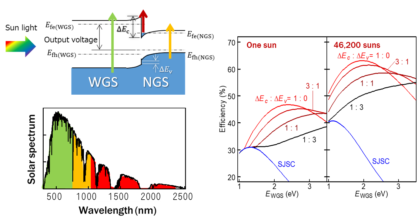
ヘテロ構造を利用したアップコンバージョン型太陽電池の概念とエネルギー変換効率予測
期待される効果や応用分野:太陽電池構造の最適化は、室内照明を利用したエネルギーの再利用やレーザーなどを利用したリモートエネルギー伝送などにも応用でき、これからのグリーン社会を支えていきます。関係する業績:“Energy Conversion Efficiency of Solar Cells” T. Kita, Y. Harada, and S. Asahi (Springer, 2019). S. Asahi, H. Teranishi, K. Kusaki, T. Kaizu, and T. Kita, Nature Communications 8, 14962 (2017).