SEARCH
検索詳細

服部 吉晃大学院工学研究科 電気電子工学専攻准教授
研究活動情報
■ 受賞- 2024年10月 神戸大学, 優秀若手研究者賞
- 2024年01月 コニカミノルタ科学技術振興財団, コニカミノルタ画像科学奨励賞
- 2023年11月 神戸大学, 工学部優秀教育賞
- 2023年06月 応用物理学会, 第70回応用物理学会春季学術講演会Poster Award
- 2019年12月 第16回薄膜材料デバイス研究会, スチューデントアワード, フルオロベンゼンチオールを電極表⾯に修飾した有機薄膜トランジスタ
- 2018年11月 第15回薄膜材料デバイス研究会, スチューデントアワード, フルオロベンゼンチオール修飾による金表面の制御と有機トランジスタ応用国内学会・会議・シンポジウム等の賞
- 2016年03月 応用物理学会, 第63回応用物理学会春季学術講演会講演奨励賞
- 2026年06月, Nano Express[査読有り]研究論文(学術雑誌)
- 2026年05月, Nanotechnology[査読有り]研究論文(学術雑誌)
- 2025年11月, Japanese Journal of Applied Physics[査読有り]研究論文(学術雑誌)
- 2025年08月, Japanese Journal of Applied Physics[査読有り]研究論文(学術雑誌)
- 2025年05月, Japanese Journal of Applied Physics[査読有り]研究論文(学術雑誌)
- 2024年12月, Japanese Journal of Applied Physics[査読有り]研究論文(学術雑誌)
- Abstract Optical microscopy with white light illumination has been employed when obtaining exfoliated monolayer hexagonal boron nitride (1L hBN) films from a large number of randomly placed films on a substrate. However, real-time observation of 1L hBN using a color camera under white light illumination remains challenging since hBN is transparent in the visible wavelength range. The poor optical constant of 1L hBN films in microphotographs is significantly improved using a Si substrate coated with a SiN x thin-film (SiN x /Si). When observing hBN thin films on SiN x /Si using a color digital camera in an optical microscope under white light illumination, the clarity of the captured color images depends on the thickness of the SiN x film (d). For real-time direct observation, the d was optimized based on quantitative chromatic studies tailored to Bayer filters of a color image sensor. Through image simulation, it was determined that the color difference between 1L hBN and the bare substrate is maximized at d = 59 or 70 nm, which was experimentally verified. The SiN x /Si with optimized d values visualized 1L hBN films without requiring significant contrast enhancement via image processing under white light illumination in real-time. Furthermore, the captured color photographs facilitate the reliable determination of the number of layers in few-layer hBN films using the contrast of the green channel of the images.IOP Publishing, 2024年06月, Nanotechnology, 35(37) (37), 375704 - 375704[査読有り]研究論文(学術雑誌)
- Abstract The surface properties of an InGaZnO4 (IGZO) layer with a monolayer formed on the surface using octadecyl phosphonic acid (ODPA) or (1H, 1H, 2H, 2H-heptadecafluorodecyl) phosphonic acid (FDPA) were investigated. Surface roughness, wettability, and work function were investigated using atomic force microscopy, water contact angle measurement, and photoelectron yield spectroscopy, respectively. The reaction time of monolayer formation on an IGZO layer was discussed based on the measured contact angle. An ODPA-monolayer formed at a slightly higher rate than an FDPA-monolayer. The work function measurement provided an estimate of the density of the molecule in the monolayer. Furthermore, the measured contact angle was used to evaluate the thermal stability of a monolayer. The evaluation suggested that annealing above 500 K causes monolayer desorption for both ODPA- and FDPA-monolayers.IOP Publishing, 2023年12月, Japanese Journal of Applied Physics, 63(1) (1), 01SP32 - 01SP32[査読有り]研究論文(学術雑誌)
- American Chemical Society (ACS), 2023年10月, ACS Applied Nano Materials[査読有り]研究論文(学術雑誌)
- Abstract Exfoliated flakes of layered materials, such as hexagonal boron nitride (hBN) and graphite with a thickness of several tens of nanometers, are used to construct van der Waals heterostructures. A flake with a desirable thickness, size, and shape is often selected from many exfoliated flakes placed randomly on a substrate using an optical microscope. This study examined the visualization of thick hBN and graphite flakes on SiO2/Si substrates through calculations and experiments. In particular, the study analyzed areas with different atomic layer thicknesses in a flake. For visualization, the SiO2 thickness was optimized based on the calculation. As an experimental result, the area with different thicknesses in a hBN flake showed different brightness in the image obtained using an optical microscope with a narrow band-pass filter. The maximum contrast was 12% with respect to the difference of monolayer thickness. In addition, hBN and graphite flakes were observed by differential interference contrast (DIC) microscopy. In the observation, the area with different thicknesses exhibited different brightnesses and colors. Adjusting the DIC bias had a similar effect to selecting a wavelength using a narrow band-pass filter.IOP Publishing, 2023年05月, Nanotechnology, 34(29) (29), 295701 - 295701[査読有り]研究論文(学術雑誌)
- Elsevier BV, 2023年01月, Thin Solid Films, 764, 139631 - 139631[査読有り]研究論文(学術雑誌)
- Abstract We propose a visualization technique for identifying an exfoliated monolayer hexagonal boron nitride (hBN) flake placed on a SiNx/Si substrate. The use of a Si substrate with a 63 nm thick SiNx film enhanced the contrast of monolayer hBN at wavelengths of 480 and 530 nm by up to 12% and −12%, respectively. The maximum contrast for the Si substrate with SiNx is more than four times as large as that for a Si substrate with a ∼90 or ∼300 nm SiO2 film. Based on the results of the reflectance spectrum measurement and numerical calculations, the enhancement is discussed.IOP Publishing, 2022年08月, Applied Physics Express, 15(8) (8), 086502 - 086502[査読有り]研究論文(学術雑誌)
- A trimethylsilyl-monolayer modified by vacuum ultraviolet (VUV) light has been investigated for use in solution-processed organic thin-film transistors (OTFTs). The VUV irradiation changed a hydrophobic trimethylsilyl-monolayer formed from hexamethyldisilazane vapor into a hydrophilic surface suitable for solution processing. The treated surface was examined via water contact angle measurement and X-ray photoelectron spectroscopy. An appropriate irradiation of VUV light enabled the formation of a dioctyl[1]benzothieno[3,2-b][1]benzothiophene (C8-BTBT) film on a modified monolayer by spin-coating. Consequently, the C8-BTBT-based OTFT with a monolayer modified for an optimal VUV irradiation time exhibited a field-effect mobility up to 4.76 cm2 V−1 s−1. The partial monolayer modification with VUV can be adapted to a variety of solution-processes and organic semiconductors for prospective printed electronics.{IOP} Publishing, 2022年06月, Japanese Journal of Applied Physics, 61({SE}) ({SE}), SE1012 - SE1012[査読有り]研究論文(学術雑誌)
- {IOP} Publishing, 2022年02月, Nanotechnology, 33(6) (6), 065702 - 065702
Abstract Hexagonal boron nitride (h-BN) is an important insulating layered material for two-dimensional heterostructure devices. Among many applications, few-layer h-BN films have been employed as superior tunneling barrier films. However, it is difficult to construct a heterostructure with ultra-thin h-BN owing to the poor visibility of flakes on substrates, especially on a metallic surface substrate. Since reflectance from a metallic surface is generally high, a h-BN film on a metallic surface does not largely influence reflection spectra. In the present study, a thin Au layer with a thickness of ∼10 nm deposited on a Si substrate with a thermally grown SiO2 was used for visualizing h-BN flakes. The thin Au layer possesses conductivity and transparency. Thus, the Au/SiO2/Si structure serves as an electrode and contributes to the visualization of an ultra-thin film according to optical interference. As a demonstration, the wavelength-dependent contrast of exfoliated few-layer h-BN flakes on the substrate was investigated under a quasi-monochromatic light using an optical microscope. A monolayer h-BN film was recognized in the image taken by a standard digital camera using a narrow band-pass filter of 490 nm, providing maximum contrast. Since the contrast increases linearly with the number of layers, the appropriate number of layers is identified from the contrast. Furthermore, the insulating property of a h-BN flake is examined using a conductive atomic force microscope to confirm whether the thin Au layer serves as an electrode. The tunneling current through the h-BN flake is consistent with the number of layers estimated from the contrast.[査読有り]研究論文(学術雑誌) - American Chemical Society ({ACS}), 2021年07月, The Journal of Physical Chemistry C, 125(27) (27), 14991 - 14999[査読有り]研究論文(学術雑誌)
- An organic semiconductor film made of diphenyl derivative dinaphtho[2,3-b:2',3'-f]thieno[3,2-b]thiophene (DPh-DNTT) has high carrier mobility. However, this mobility may be greatly affected by the crystal orientation of the DPh-DNTT's first layer. Polarization Raman microscopy is widely used to quantitatively analyze the molecular orientation, and thus holds great potential as a powerful tool to investigate the crystal orientation of monolayer DPh-DNTT with high spatial resolution. In this study, we demonstrate polarization Raman imaging of monolayer DPh-DNTT islands for crystal orientation analysis. We found that the DPh-DNTT sample indicated a strong dependence of the Raman intensity on the incident polarization direction. Based on the polarization dependence, we developed an analytical method of determining the crystal orientation of the monolayer DPh-DNTT islands and experimentally confirmed that our technique was highly effective at imaging the islands' crystal orientation with a spatial resolution of a few hundred nanometers.2021年04月, ACS omega, 6(14) (14), 9520 - 9527, 英語, 国際誌[査読有り]研究論文(学術雑誌)
- 2020年12月, JOURNAL OF PHYSICS D-APPLIED PHYSICS, 53(50) (50), 英語[査読有り]研究論文(学術雑誌)
- The initial stage of organic semiconductor film formation greatly affects the properties of films, which are used in organic devices including thin-film transistors and light-emitting diodes. Organic monolayer islands that are formed on a suitable substrate can be observed with a conventional optical microscope. Furthermore, the use of a polarized microscope allows the determination of the refractive index and crystal orientation of islands. Here, we report organic monolayer islands of 2,9-diphenyl-dinaphtho[2,3-b:2',3'-f]thieno[3,2-b]thiophene (DPh-DNTT) deposited on a Si substrate with thermally grown SiO2 to investigate the crystal orientation of islands by polarized light microscopy. The observation of DPh-DNTT islands under polarized quasi-monochromatic light reveals that reflection intensity depends on both the crystal orientation and irradiation wavelength. A comparison between experimental and calculated reflection intensities provides an estimate of an anisotropic complex refractive index in the plane. The crossed-polarized microscopy image of a SiO2/Si substrate with DPh-DNTT islands shows that the contrast between the islands and SiO2 surface is sensitive to the angle between the polarizer and analyzer and depends on the direction of crystal orientation. The dependence of reflection contrast, which can be explained by the anisotropic extinction coefficient, is used to confirm crystal orientation.American Chemical Society (ACS), 2020年08月, ACS applied materials & interfaces, 12(32) (32), 36428 - 36436, 英語, 国際誌[査読有り]研究論文(学術雑誌)
- 2020年03月, JAPANESE JOURNAL OF APPLIED PHYSICS, 59(3) (3), 036503 - 036503, 英語[査読有り]研究論文(学術雑誌)
- 2020年03月, JAPANESE JOURNAL OF APPLIED PHYSICS, 59(SD) (SD), SDDA09 - SDDA09, 英語[査読有り]研究論文(学術雑誌)
- 2020年03月, JAPANESE JOURNAL OF APPLIED PHYSICS, 59(SD) (SD), SDDA03 - SDDA03, 英語[査読有り]研究論文(学術雑誌)
- 2020年03月, FLEXIBLE AND PRINTED ELECTRONICS, 5(1) (1), 英語[査読有り]研究論文(学術雑誌)
- 2020年01月, JOURNAL OF PHYSICAL CHEMISTRY C, 124(1) (1), 1064 - 1069, 英語[査読有り]研究論文(学術雑誌)
- 2019年11月, ORGANIC ELECTRONICS, 74, 245 - 250, 英語[査読有り]研究論文(学術雑誌)
- 2019年10月, DATA IN BRIEF, 26, 104522 - 104522, 英語, 国際誌[査読有り]研究論文(学術雑誌)
- 2019年04月, JAPANESE JOURNAL OF APPLIED PHYSICS, 58(SB) (SB), SBBJ04, 英語[査読有り]研究論文(学術雑誌)
- 2018年04月, ACS APPLIED MATERIALS & INTERFACES, 10(14) (14), 11732 - 11738, 英語, 国際誌[査読有り]研究論文(学術雑誌)
- 2018年01月, PHYSICAL REVIEW B, 97(4) (4), 045425, 英語[査読有り]研究論文(学術雑誌)
- Electrochemical Society Inc., 2017年, ECS Transactions, 79(1) (1), 91 - 97, 英語[査読有り]研究論文(国際会議プロシーディングス)
- 2016年12月, APPLIED PHYSICS LETTERS, 109(25) (25), 253111, 英語[査読有り]研究論文(学術雑誌)
- 2016年10月, ACS APPLIED MATERIALS & INTERFACES, 8(41) (41), 27877 - 27884, 英語, 国際誌[査読有り]研究論文(学術雑誌)
- 2015年12月, 2D MATERIALS, 2(4) (4), 041002, 英語[査読有り]研究論文(学術雑誌)
- 2015年01月, ACS NANO, 9(1) (1), 916 - 921, 英語, 国際誌[査読有り]研究論文(学術雑誌)
- 2014年10月, ADVANCED HEALTHCARE MATERIALS, 3(10) (10), 1597 - 1607, 英語, 国際誌[査読有り]研究論文(学術雑誌)
- 2014年02月, NATURE COMMUNICATIONS, 5, 3266 - 3266, 英語, 国際誌[査読有り]研究論文(学術雑誌)
- 2013年11月, JOURNAL OF ALLOYS AND COMPOUNDS, 578, 148 - 152, 英語[査読有り]研究論文(学術雑誌)
- 2013年08月, CURRENT APPLIED PHYSICS, 13(6) (6), 1050 - 1054, 英語[査読有り]研究論文(学術雑誌)
- 2013年05月, JOURNAL OF ALLOYS AND COMPOUNDS, 560, 105 - 110, 英語[査読有り]研究論文(学術雑誌)
- 2012年01月, SURFACE & COATINGS TECHNOLOGY, 206(8-9) (8-9), 2140 - 2145, 英語[査読有り]研究論文(学術雑誌)
- 2011年12月, MATERIALS CHEMISTRY AND PHYSICS, 131(1-2) (1-2), 425 - 430, 英語[査読有り]研究論文(学術雑誌)
- 2011年01月, MATERIALS LETTERS, 65(2) (2), 188 - 190, 英語[査読有り]研究論文(学術雑誌)
- 2010年07月, INTERNATIONAL JOURNAL OF HEAT AND MASS TRANSFER, 53(15-16) (15-16), 3067 - 3074, 英語[査読有り]研究論文(学術雑誌)
- 2010年03月, JOURNAL OF APPLIED PHYSICS, 107(6) (6), 063305 - 063308, 英語[査読有り]研究論文(学術雑誌)
- “In-liquid plasma” is generated inside the bubbles on the tip of an electrode by applying microwave radiation from the electrode. The in-liquid plasma on the tip of an electrode consists of a plasma generation region, vapor phase, bubble interface, and liquid phase. The growth of the bubble, including the plasma, in n-dodecane was observed using a high-speed camera. This was done because the pressure and the temperature surrounding the plasma needed to be clarified for utilizing it in such processes as chemical vapor deposition. The dependence of the bubble growth on the vessel pressure and on the microwave power was clarified, and the internal pressure of the bubbles was calculated by substituting the approximation curve of the observed bubble diameter in the Rayleigh-Plesset equation. The bubbles grow not continuously but intermittently as the plasma region expands and contracts. The growth of the bubbles increases with increase in the microwave power or decrease in the vessel pressure. The value of the internal pressure of the bubbles peaks between 200 and 600 hPa, it increases as the microwave power increases, and the effect of the vessel pressure on it is small. In addition, we measured the temperature surrounding the plasma using a thermocouple. The temperature can be measured vertically from the vapor phase to the liquid phase by moving the thermocouple in that direction. The point where the temperature measurable by the thermocouple reaches a maximum moves away from the tip of the electrode as the microwave power increases. The maximum temperature reaches the approximate saturation temperature of the liquid.社団法人 日本伝熱学会, 2008年10月, 伝熱 : journal of the Heat Transfer Society of Japan, 47(201) (201), 131 - 137, 日本語[査読有り]研究論文(学術雑誌)
- 単著, 月刊OPTRONICS (オプトロニクス社) 44(520), 2025年04月無反射多層基板を用いた光学的精密計測
- 単著, JSAP Review(応用物理学会), 240406, 2024年Substrates for enhancing contrast in optical microscope images of layered materials.
- 光学 (日本光学会), 53, 256, 2024年透明な極薄膜を光学顕微鏡で観察するための無反射基板
- 応用物理 (応用物理学会), 93, 231-235, 2024年層状物質の光学顕微鏡像におけるコントラストを増強するための基板
- 共著, NEW DIAMOND (ニューダイヤモンドフォーラム), 133,19-24, 2019年, 日本語BNの絶縁性破壊強さの異方性とその起源学術書
- ケミカルエンジニアリング (化学工業社), 57(7), 548-553, 2012年液中プラズマによるナノ粒子製造方法
- 第73回応用物理学会春季学術講演会, 2026年03月pチャネル薄膜トランジスタ特性向上に向けたポストアニールによるSnOx薄膜の相変化
- 第73回応用物理学会春季学術講演会, 2026年03月白色照明を用いた極薄膜顕微イメージングに適した無反射多層基板
- 応用物理学会関西支部2025年度第2回講演会, 2025年11月多層構造の基板を用いたアルミニウム表面酸化過程の光学的高感度検出
- 応用物理学会関西支部2025年度第2回講演会,, 2025年11月ホスホン酸単分子膜を形成した酸化ニッケルの表面物性制御
- 44th Electronic Materials Symposium, 2025年10月Post-annealing effects on p-channel SnOx thin-film transistors fabricated by reactive sputtering using a Sn target
- 第86回応用物理学会秋季学術講演会, 2025年09月有機単分子膜を粘着層に用いた金薄膜の結晶構造評価
- The 10th Int. Sym. on Organic and Inorganic Electronic Materials and Related Nanotechnologies, 2025年06月Formation of a phosphonic acid monolayer on an In5GaZnO10 thin film
- The 10th Int. Sym. on Organic and Inorganic Electronic Materials and Related Nanotechnologies, 2025年06月Hydrophilic/hydrophobic patterning for controlling droplet dynamics
- The 10th Int. Sym. on Organic and Inorganic Electronic Materials and Related Nanotechnologies, 2025年06月Post-annealing effect in p-channel thin-film transistors with SnOx as the channel layer
- 第72回応用物理学会春季学術講演会, 2025年03月極薄膜イメージングのための有機単分子膜を用いた無反射基板の作製
- コニカミノルタカレッジ, 2024年12月無反射多層基板を用いた極薄膜の検出と設計方法[招待有り]
- 応用物理学会関西支部 2024年度第2回講演会, 2024年11月有機単分子膜による親水・疎水パターンの形成と無反射多層基板を用いた可視化
- JST-神戸大学 新技術説明会, 2024年10月無反射多層基板を用いた光学的精密計測[招待有り]
- 第43回電子材料シンポジウム, 2024年10月移動度 1 cm2 V-1 s-1 を超える SnOx pチャネル薄膜トランジスタ
- 第43回電子材料シンポジウム, 2024年10月真空中および大気中で極薄膜InGaZnOトランジスタの電流電圧特性
- 第85回応用物理学会学術講演会, 2024年09月p チャネルSnOx 薄膜トランジスタのポストアニール効果
- 第85回応用物理学会学術講演会, 2024年09月真空中における極薄膜InGaZnO トランジスタの電流電圧特性
- 第71回応用物理学会春季学術講演会, 2024年03月窒化膜付きシリコン基板を用いた単層hBNの観察口頭発表(一般)
- 薄膜材料デバイス研究会第20回研究集会, 2023年11月フォトマスクを用いた酸化金のパターニング形成ポスター発表
- 薄膜材料デバイス研究会第20回研究集会, 2023年11月光電子収量分光法によるIn7GaZnO13薄膜の仕事関数測定ポスター発表
- 薄膜材料デバイス研究会第20回研究集会, 2023年11月二層構造InGaZnO4/In5GaZnO10から成る薄膜トランジスタの特性評価ポスター発表
- 薄膜材料デバイス研究会第20回研究集会, 2023年11月光学顕微鏡を用いたチオール有機単分子膜のパターニング評価ポスター発表
- 神戸大学大学院工学研究科先端膜工学研究拠点第9回ワークショップ, 2023年10月無反射多層基板を用いた二次元材料と有機単分子膜の可視化[招待有り]
- The 9th International Symposium on Organic and Inorganic Electronic Materials and Related Nanotecnologies (EM-NANO 2023), 2023年06月Coverage control of a phosphonic acid monolayer on an InGaZnO surfaceポスター発表
- 第70回応用物理学会春季学術講演会, 2023年03月有機薄膜形成のためのインクジェット法による親水疎水パターニングを用いた液摘挙動制御
- 第70回応用物理学会春季学術講演会, 2023年03月スパッタリングにより作製したIn5GaZnO10薄膜トランジスタの特性評価
- 第70回応用物理学会春季学術講演会, 2023年03月層状物質の厚い膜に存在する単層分の厚さの違いを検知する手法
- 第83回応用物理学会秋季学術講演会, 2022年09月大気中光電子収量分光法による原子比率の異なるInGaZnO 薄膜の仕事関数評価
- 第83回応用物理学会秋季学術講演会, 2022年09月In5GaZnO10薄膜トランジスタの特性評価
- 第83回応用物理学会秋季学術講演会, 2022年09月塗布型有機薄膜トランジスタのためのUV/オゾン処理による有機単分子膜の改質
- 第83回応用物理学会秋季学術講演会, 2022年09月六方晶窒化ホウ素の高電界下における電気伝導と絶縁破壊[招待有り]
- 第69回応用物理学会春季学術講演会, 2022年03月大気中光電子収量分光法によるInGaZnO薄膜のエネルギーバンド構造解析ポスター発表
- 第69回応用物理学会春季学術講演会, 2022年03月金極薄膜を用いた単層h-BNの可視化口頭発表(一般)
- 2021 MRS FALL MEETING, 2021年12月Organic thin-film transistors for high performance logic circuits: Realization of short channel, high mobility, low contact resistance and threshold voltage control[招待有り]
- 薄膜材料デバイス研究会 第18回研究集会, 2021年11月金属顕微鏡を用いたアルカンチオール単分子有機膜の可視化
- 応用物理学会関西支部 2021年度第2回講演会, 2021年10月塗布法による有機半導体薄膜の製膜において 2度塗りした際の薄膜形成メカニズム
- 応用物理学会関西支部 2021年度第2回講演会, 2021年10月疎水性単分子膜を修飾した基板上への塗布法を用いた有機半導体薄膜形成技術
- The International Conference on Flexible and Printed Electronics (ICFPE), 2021年09月Organic monolayers modified by ultraviolet-ozone for solution-processed organic thin-film transistors
- 応用物理学会関西支部 2021年度第1回講演会, 2021年04月光学顕微鏡による的異方性を持つ単分子有機薄膜の観察と画像処理解析
- 応用物理学会関西支部 2021年度第1回講演会, 2021年04月光電子収量分法による酸素プラズマ処理したSiO2絶縁膜表面のエネルギー準位分析
- 応用物理学会関西支部 2021年度第1回講演会, 2021年04月撥水性基板上にスピンコート法を用いて作製した有機薄膜トランラジタの評価
- IEEE EDS Kansai Chapter 第20回「関西コロキアム電子デバイスワークショップ」, 2020年11月Bottom-contact pentacene thin-film transistor with threshold voltages controlled by oxygen plasma treatment
- 薄膜材料デバイス研究会 第17回研究集会, 2020年11月酸素プラズマ処理により生じる有機半導体/ゲート絶縁膜界面準位のエネルギー分布
- 39th Electronic Materials Symposium, 2020年10月Highly thermal-stable monolayers formed on a gold surface using benzenedithiol
- 39th Electronic Materials Symposium, 2020年10月Evaluation of carrier mobility in organic metal-oxide-semiconductor capacitors
- 第67回応用物理学会春季学術講演会, 2020年03月偏光顕微鏡を用いた単層DPh-DNTT二次元核の方位決定
- 第67回応用物理学会春季学術講演会, 2020年03月酸素プラズマ処理が与える有機半導体/絶縁膜界面準位への影響
- 薄膜材料デバイス研究会 第16回研究集会, 2019年11月フルオロベンゼンチオールを電極表面に修飾した有機薄膜トランジスタ
- 38th Electronic Materials Symposium, 2019年10月Statistical study of shape for submonolayer 2D islands of DPh-DNTT prepared by vacuum deposition
- 第80回応用物理学会学術講演会, 2019年09月金表面に形成したベンゼンジチオール単分子膜の耐熱性評価
- 第80回応用物理学会学術講演会, 2019年09月MOSキャパシタ構造を利用した有機半導体中のキャリア移動度評価
- 第80回応用物理学会学術講演会, 2019年09月単層 DPh-DNTT の2次元アイランドにおける異方性
- International Conference on Solid State Devices and Materials (SSDM), 2019年09月Bottom-contact pentacene thin-film transistor with threshold voltages controlled by oxygen plasma treatment
- 応用物理学会関西支部 2019年度第1回講演会, 2019年06月有機薄膜トランジスタにおける酸素プラズマを用いたパターニング
- 応用物理学会関西支部 2019年度第1回講演会, 2019年06月UV/ozone処理を用いた熱酸化膜上単分子膜の被覆率操作
- 10th International Conference on Molecular Electronics and Bioelectronics (M&BE 10), 2019年06月The formation of a mixed monolayer on a gold surface toward surface property control
- 10th International Conference on Molecular Electronics and Bioelectronics (M&BE 10), 2019年06月High thermal stability of the benzenedithiol monolayer formed on a gold surface
- 10th International Conference on Molecular Electronics and Bioelectronics (M&BE 10), 2019年06月Surface properties of oriented polytetrafluoroethylene films with a micrometer pitch
- Compound Semiconducotr Week (csw2019), 2019年05月, 英語, 国際会議Voltage and frequency dependence of capacitance characteristics in organic MOS capacitorsポスター発表
- Compound Semiconducotr Week (csw2019), 2019年05月, 英語, 国際会議Thin-film transistors based on copper phthalocyanine deposited on a gate dielectric rubbed with poly(tetrafluoroethylene)ポスター発表
- Compound Semiconducotr Week (csw2019), 2019年05月, 英語, 国際会議Nucleation and shape of 2D islands of DPh-DNTT thin-films prepared by vacuum evaporation口頭発表(一般)
- 第67応用物理学関係連合講演会, 2019年03月酸素プラズマ処理が与える有機半導体/絶縁膜界面準位への影響
- 第67応用物理学関係連合講演会, 2019年03月偏光顕微鏡を用いた単層DPh-DNTT二次元核の方位決定
- 第66回応用物理学会春季学術講演会, 2019年03月, 日本語, 国内会議有機MOSキャパシタの電圧・周波数特性解析口頭発表(一般)
- 第66回応用物理学会春季学術講演会, 2019年03月, 日本語, 国内会議真空蒸着法におけるDNTTとその誘導体の核形成機構口頭発表(一般)
- 第66回応用物理学会春季学術講演会, 2019年03月, 日本語, 国内会議酸素プラズマ処理によるボトムコンタクト型有機トランジスタの閾値電圧制御ポスター発表
- 第15回薄膜材料デバイス研究会, 2018年11月, 日本語, 国内会議ポリテトラフルオロエチレン配向膜を有する銅フタロシアニン薄膜トランジスタポスター発表
- 第15回薄膜材料デバイス研究会, 2018年11月, 日本語, 国内会議フルオロベンゼンチオール修飾による金表面の制御と有機トランジスタ応用口頭発表(基調)
- 第79回応用物理学会学術講演会, 2018年09月, 日本語, 国内会議有機薄膜トランジスタへの応用に向けたフルオロベンゼンチオール表面修飾による金電極の仕事関数制御ポスター発表
- 第79回応用物理学会学術講演会, 2018年09月, 日本語, 国内会議有機薄膜トランジスタにおける酸素プラズマ処理による閾値電圧シフトの起源ポスター発表
- 第79回応用物理学会学術講演会, 2018年09月, 日本語, 国内会議真空蒸着法におけるDPh-DNTT薄膜の成長機構口頭発表(一般)
- International Conference on Solid State Devices and Materials (SSDM), 2018年09月, 英語, 国際会議Logic circuits consisting of pentacene thin-film transistors with controlled threshold voltages口頭発表(一般)
- International Conference on Solid State Devices and Materials (SSDM), 2018年09月, 英語, 国際会議Growth mechanism and electrical characterization of DPh-DNTT films prepared by vacuum deposition口頭発表(一般)
- 2nd Bilateral Kobe-Kiel Workshop, 2018年09月, 英語, 国際会議Dielectric breakdown of h-BN and growth mechanism of DPh-DNTT口頭発表(一般)
- 3rd Bilateral Workshop on Research Exchange between National Taiwan University and Kobe University, 2018年07月, 英語, 国際会議Thermal resistivity of copper phthalocyanine based thin-film transistorsポスター発表
- 3rd Bilateral Workshop on Research Exchange between National Taiwan University and Kobe University, 2018年07月, 英語, 国際会議Layered materials for electronics口頭発表(一般)
- 3rd Bilateral Workshop on Research Exchange between National Taiwan University and Kobe University, 2018年07月, 英語, 国際会議Electrode-surface modification for high-performance organic thin-film transistorsポスター発表
- 第65応用物理学関係連合講演会, 2018年03月, 日本語, 国内会議ボトムコンタクト型有機薄膜トランジスタにおける閾値電圧制御ポスター発表
- 第65応用物理学関係連合講演会, 2018年03月, 日本語, 国内会議キャパシタンス測定による有機トランジスタの寄生抵抗評価口頭発表(一般)
- 第65回応用物理学会春季学術講演会, 2018年03月, 日本語, 国内会議DPh-DNTT 薄膜トランジスタの遮断周波数測定ポスター発表
- 2016 COMPOUND SEMICONDUCTOR WEEK (CSW) INCLUDES 28TH INTERNATIONAL CONFERENCE ON INDIUM PHOSPHIDE & RELATED MATERIALS (IPRM) & 43RD INTERNATIONAL SYMPOSIUM ON COMPOUND SEMICONDUCTORS (ISCS), 2016年, 英語, IEEEDielectric breakdown of layered insulator
- 中国四国支部総会・講演会 講演論文集, 2012年, 日本語, 一般社団法人 日本機械学会1317 水-メタノール混合溶液中でのマイクロ波プラズマによる生成気体に関する研究(熱工学III)
- 中国四国支部総会・講演会 講演論文集, 2012年, 日本語, 一般社団法人 日本機械学会1314 マイクロ波液中プラズマを利用したナノ粒子の連続合成と圧力の影響(熱工学III)
- 中国四国支部総会・講演会 講演論文集, 2011年, 日本語, 一般社団法人 日本機械学会1407 液中プラズマ化学蒸着によるダイヤモンドの生成に適する基板の検討(熱工学II)
- 中国四国支部総会・講演会 講演論文集, 2011年, 日本語, 一般社団法人 日本機械学会1408 液中プラズマ化学蒸着法におけるダイヤモンドの最適生成条件の検討(熱工学II)
- 日本伝熱シンポジウム講演論文集, 2011年, 日本語, 社団法人 日本伝熱学会, 液体中で亜鉛の電極を利用しマイクロ波プラズマを発生させて電極を原料としたナノ粒子の合成を行った。エタノール中でプラズマを発生させると10-200nmの六角柱または球体の亜鉛ナノ粒子が合成され、純水中で発生させると亜鉛ナノ粒子と酸化亜鉛ナノ粒子が凝集した約200nmの花びら型をした粒子が合成された。また、電極上部に設置された金属プレートの直径と位置を変え、ナノ粒子の合成に及ぼす影響を調べた。ナノ粒子の合成速度は金属プレートの直径が大きいほど、位置が電極先端に近いほど大きくなった。投入電力が230Wの場合、合成速度は5g/hourとなった。さらに、銅の電極を利用し放電開始電力を調べた。放電開始電力は金属プレートの位置が近いほど小さくなった。マイクロ波液中プラズマを利用したナノ粒子の合成と対向プレートの影響
- 日本機械学会中国四国支部・九州支部合同企画講演会講演論文集, 2010年10月, 日本語二層誘電体同軸型電極を利用したマイクロ波液中プラズマ
- 日本機械学会中国四国支部・九州支部合同企画講演会講演論文集, 2010年10月, 日本語液中プラズマ化学蒸着におけるプラズマ泡と基板の相互作用
- 日本伝熱シンポジウム講演論文集, 2010年, 日本語, 社団法人 日本伝熱学会, 純水中に発生するマイクロ波液中プラズマの点火位置を高速度カメラで観察した。また、3D-FDTD法を用いて電極表面の電界を計算し、マイクロ波によって加熱される液体が吸収する熱量を計算した。この熱量を使って電極周辺の液体の温度計算した結果、プラズマが発生する電極表面の電界強度の最も高い位置と、最も温度が高い位置は必ずしも一致しないことが明らかになった。また、実験から測定したプラズマの点火位置と数値計算によって求めた最も温度の高い地点が一致した。マイクロ波液中プラズマの点火位置に対する熱的影響
- 中国四国支部総会・講演会 講演論文集, 2009年, 日本語, 一般社団法人 日本機械学会403 マイクロ波液中プラズマの電極形状が放電開始条件に及ぼす影響(熱工学I)
- 日本伝熱シンポジウム講演論文集, 2009年, 日本語, 社団法人 日本伝熱学会, 純水中に高周波を照射する電極を設置し,電極先端でプラズマを発生させる.高速度カメラでプラズマを内包する気泡の挙動を観察する.気泡の生成様式は,水温と供給電力により4つに分類され,加熱沸騰の場合との比較を行った.供給電力に対して,水温の上昇に消費される熱は約90%,蒸発として消費される熱は約10%,気泡表面から水中へと伝導される熱は約30%,さらに,化学反応により消費される熱は1%以下となることがわかった.水中プラズマによる気泡発生様式と熱収支
- HT2008: PROCEEDINGS OF THE ASME SUMMER HEAT TRANSFER CONFERENCE, VOL 1, 2009年, 英語, AMER SOC MECHANICAL ENGINEERS, The plasma in liquid is generated by applying High-Frequency (HF) irradiation of 27.12 MHz or Microwave (MW) irradiation of 2.45 GHz from an electrode, namely, a monopole-antenna electrode inserted into a reactor vessel. n-dodecane, methanol, and water are used as test liquids. The glow discharge plasma can be kept in spite of atmospheric pressure due to the cooling effect of liquid itself The light emission from the plasma changes substantially according to the behavior of the bubble. The present Chemical Vapor Deposition (CVD) process also enabled simultaneous production of hydrogen gas and the synthesis of the Carbon Nano-Tubes (CNTs) in hydrocarbon liquids. The actual production of hydrogen per unit energy by this process corresponds to approximately 1% of that by conventional steam reforming method and about 32% of that by the alkaline water electrolysis. Moreover, this process can make the solid carbon of about 14 g/h at the same time.Simultaneous Production of Hydrogen and CNTs by In-Liquid Plasma, and Its Discharge Characteristics
- 日本伝熱シンポジウム講演論文集, 2008年, 日本語, 社団法人 日本伝熱学会, 液中プラズマは気相プラズマとは異なる特徴をもち,応用研究は活発に行われている.一方,基礎的な発生メカニズムや物性に関する研究報告は少ない.本研究では,プラズマ発生と同時に,プラズマを内包しながら発生し成長する泡の挙動を高速度ビデオカメラで撮影し,画像から気泡内部の圧力を求め,熱電対を用いてプラズマ周辺の温度を測定する.液中プラズマの気泡は系圧力が小さいほど大きく成長し,気泡が膨張,収縮する周期が長くなる.周辺温度はプラズマが消費するエネルギー量が大きく,系圧力が大きいほど上昇する.液中プラズマの気泡の挙動と周辺温度
- 日本伝熱シンポジウム講演論文集(CD-ROM), 2007年, 日本語有機溶媒中におけるマイクロ波プラズマの挙動特性
- IEEE EDS Kansai Chapter 第19回「関西コロキアム電子デバイスワークショップ」Logic Circuits Consisting of Pentacene Thin-Film Transistors with Controlled Threshold Voltages
- 日本学術振興会, 科学研究費助成事業, 基盤研究(B), 神戸大学, 2024年04月 - 2028年03月ヘテロ接合型薄膜デバイスへの応用に向けた酸化インジウム化合物のバンド構造制御
- 日本学術振興会, 科学研究費助成事業, 基盤研究(C), 神戸大学, 2024年04月 - 2027年03月有機薄膜形成のための親水疎水パターニングを利用した液滴の動的制御
- NEDO, 官民による若手研究者発掘支援事業, 神戸大学, 2024年10月 - 2026年09月, 研究代表者光学顕微鏡像における垂直方向の分解能を向上させるための無反射多層基板の開発
- 日本学術振興会, 科学研究費助成事業 基盤研究(C), 基盤研究(C), 神戸大学, 2021年04月 - 2024年03月その場観察法を用いた有機半導体薄膜の成長メカニズムの解明フレキシブルデバイスやウェアラブルデバイスを実現するためには、熱に弱い柔軟なフィルム上にトランジスタを安価に作製する技術が必要である。近年、安価で大面積に有機トランジスタを作成する新しい手法として、有機溶媒に有機半導体材料を溶かした溶液をインクとして、印刷技術により基板に塗布し、有機半導体薄膜を製膜する手法が注目されている。この手法では基板に溶液を塗り広げて溶媒を乾燥させることで製膜するため、原理上、親水性の基板が望ましい。しかし、一般的に親水性基板の表面にはトランジスタのキャリア移動度を低下させるキャリアトラップが多数あることから、電子デバイスの観点としては疎水性基板が望ましく、これらを両立することは困難である。そこで、本研究では疎水性の基板を親水化するプロセスの処理時間に着目し、溶液の塗布が可能な最低限の処理を基板に行うことを提案し、検証した。撥水性基板として、絶縁膜の表面に有機単分子膜を製膜し、UVオゾン処理を行うことで親水化させる。有機薄膜はスピンコート法により溶液から製膜した。作製した薄膜を用いて有機トランジスタを作成し、電気特性の評価を行ったところ、UVオゾン処理時間を適切に制御することで、最大で4.76 cm2/(Vs)のキャリア移動度をもつ有機トランジスタが作製された。この値は過去の文献と比較しても、親水性基板を利用し、スピンコート法で作成されたトランジスタとしてはかなり高く、親水性かつトラップサイトの少ない、理想的な界面が形成された可能性がある。有機単分子膜の一部を親水化させる本手法は塗布型有機半導体トランジスタの作成において汎用的に適応可能な技術であり、実用化への貢献が期待される。
- 日本学術振興会, 科学研究費助成事業 基盤研究(B), 基盤研究(B), 神戸大学, 2019年04月 - 2022年03月分子配向/界面制御に基づく高性能有機トランジスタ実現のための基盤技術開発本研究では実用に耐えうる低電圧,高速動作可能な有機トランジスタの開発を目指して,それを実現するための基盤技術開発に取り組んでいる.特に,[A]有機薄膜の配向性,[B]金属表面の単分子膜,[C]酸化物の表面処理とドーピング,[D]有機半導体へのドーピング,[E]顕微ラマン分光に関わる技術を駆使して,目標とする特性を実現することを目指している.[A]有機薄膜の配向性については,高移動度かつ熱耐性にすぐれるDPh-DNTTという材料について,真空蒸着の際にlayer-by-layer成長をすることを確認し,かつ,高移動度化に有利となる大きなグレインが得られる条件を見出した.また,配向制御に利用するテフロン板をつかったラビング膜の作製も開始し,最適な条件を見しだしつつある.[B]金属表面の単分子膜については,量子化学計算により予測した,分極の大きい分子を表面修飾に用いることにより,より広い範囲で仕事関数を制御することに成功した.[C]酸化物の表面処理とドーピングについては,酸素プラズマ処理による閾値電圧制御について,シリコン熱酸化膜の価電子帯上端付近に,エネルギー準位が形成することを見出した.[D]有機半導体へのドーピングはフェルミ準位制御を目的としているが,フェルミ準位の測定に向けて,閾値電圧制御した有機MOSキャパシタのインピーダンス分光に取り組んでおり,測定方法を確立しつつある.[E]顕微ラマン分光については,まずは,DPh-DNTT薄膜の測定に取り組み,膜厚に依存してラマンスペクトルの強度が変化することを確認した.また,量子化学計算により予測されるピークとの対応付を行った.
- 日本学術振興会, 科学研究費助成事業 若手研究, 若手研究, 神戸大学, 2019年04月 - 2021年03月多結晶有機半導体薄膜におけるキャリア散乱と輸送特性の向上に関する研究有機半導体デバイスの実用化にはキャリア移動度の向上が必要である。移動度の低下は結晶粒界で起こるため、デバイスの有機半導体層の粒界を少なくすることが有効であるが、今だ、商用利用可能な技術は確立されていない。真空蒸着法は現状の半導体シリコンデバイスでも使われている一般的な薄膜の作製方法であり、有機半導体薄膜への技術転用が容易であるが、真空蒸着法では有機半導体薄膜が多結晶膜になってしまうので、結晶粒を大きくする蒸着手法を見出すことが重要である。結晶粒は結晶核から成長するので、製膜開始直後の結晶核の核密度を減少し、形成過程を制御することが重要であるため、薄膜の初期成長に関して調査を行った。 有機半導体デバイスに使われる低分子材料は基板から層状に一層ずつ成長していく性質があるが、1層目が完成する前に蒸着を止めて、その形や密度を調べた。結晶核の密度は、蒸着前の基板の表面処理や蒸着中の基板温度により変わることが分かった、一方で、蒸着条件にかかわらず、結晶核の形は核密度が減少するほどフラクタル状に複雑な形になった。これらは基板に到達した有機分子が基板の表面で起こす表面拡散と、既存の安定した結晶核に取り込まれた有機分子が核の周囲を拡散するエッジ拡散によって説明が可能である。表面拡散が大きいほど核密度が減少し、エッジ拡散が大きいほど単純な形の結晶核が形成される。様々な蒸着条件で実験を繰り返し、これらの関係を分析した結果、エッジ拡散は基板の表面処理に依存しないことが分かり、材料固有のもつ物性値のようにみなせることが分かった。デバイス応用を考える上では、エッジ拡散は大きい方が好ましく、これらの値は分子間の相互作用によって決まるために、近年研究が進んでいる細長い棒状の低分子の構造において、エッジ拡散の観点から骨格や側鎖の材料設計を行うことが重要であると考えられる。
- 日本学術振興会, 学術研究助成基金助成金/若手研究(B), 若手研究(B), 神戸大学, 2017年04月 - 2019年03月, 研究代表者高い電子移動度を持つグラフェン電界効果トランジスタは、六方晶窒化ホウ素(h-BN)の上に設置することにより、さらに性能が向上することが分かっている。しかし、h-BNをゲート絶縁膜として利用する場合、誘電率が低い問題がある。この問題はh-BNを薄くして、高い誘電率を持つ材料に積層させることで解決できるが、h-BNを薄くした際に流れるリーク電流の調査が必要である。本研究ではそのリーク電流がホール電流であることを明らかにし、それを電極の材料により抑制できることを実験的に確かめた。競争的資金
- 日本学術振興会, 科学研究費助成事業 研究活動スタート支援, 研究活動スタート支援, 東京大学, 2014年08月 - 2016年03月層状絶縁物質であるh-BNはグラフェンFETのゲート絶縁膜や積層型電子デバイスの基板として理想的な物質として広く認識されているものの、絶縁膜としての信頼性や破壊メカニズムは未解明であるので、絶縁性に関して基礎研究を行った。本研究では、特に結晶構造に起因した破壊の異方性に着目して研究を行った。c軸に平行な方向における絶縁破壊強さをコンダクティブAFMを使って測定すると12 MV/cmであり、既存のアモルファスシリコン酸化物に匹敵することがわかった。一方、h-BNの表面に電極を作成しc軸に垂直方向の破壊強さを測定すると、3MV/cm程度であり、破壊電界に異方性があることを明らかにした。
研究シーズ
■ 研究シーズ- 極薄膜や表面吸着物を光学的に顕微評価を行う研究シーズカテゴリ:ナノテク・材料, エネルギー, 自然科学一般研究キーワード:電子デバイス, 表面, 単分子膜, センサー研究の背景と目的:厚さ数nmの極薄膜を簡便に顕微評価をする手法を開発しています。既存の技術において極薄膜はX線や電子線、原子間力顕微鏡、エリプソメーターなどを駆使して複合的に評価を行いますが、いずれの手法も簡便で安価な方法とは言えません。一方で、光学的な干渉効果を用いれば、大面積かつ、迅速に、非破壊で、室温大気圧下で評価することが可能です。研究内容:有機材料を用いた電子デバイスでは、有機薄膜の質や材料の界面がデバイスの性能に大きく影響するので、本技術を用いて性能のよいデバイスを開発しています。例えば、材料の表面に意図的に有機物を付着させて界面を改質する手法があります。その様な極薄膜は通常、可視性が乏しく、その存在すら確認することはできません。下記の左の図は本手法の一例として、金基板の表面に異なる有機分子を表面に吸着させて、カメラで並べて撮影した写真です。色の違いは分子の大きさの違いを示しています。条件によっては、薄膜の平均厚さとして、0.1nm程度の高さの違いを検出することができます。また、偏光によって観察を行うことで、薄膜の結晶性も評価できます。下記の図の右の写真2枚は、基板上に製膜された厚さ2nmの単分子有機薄膜の成長過程を示しています。薄膜が円形に成長する様子が明確に認知でき、赤と青線は結晶軸を示しています。
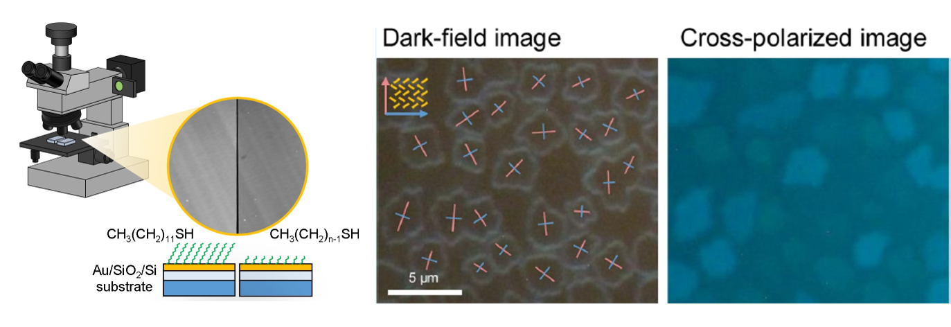
異なる有機物で改質した2枚の基板の観察(左)と円形に成長している単分子有機薄膜(右)
期待される効果や応用分野:本手法は極薄膜のみならず、基板の表面に付着する吸着物や、表面のわずかな化学的、物理的経時変化も検出することができます。通常、極薄膜は直接見ることができないので、どのように反応が進んでいるかを判断するのは困難です。本手法は一般的な金属顕微鏡で薄膜を観察し、カメラで撮影するだけで、水平方向に1μm程度の分解能で、この変化を直接観測することができるので、幅広い分野で、応用が可能だと考えられます。
hattori eedept.kobe-u.ac.jp ※左記の「@」は画像ですので、ご利用の際はテキストの「@」を入力してください。
eedept.kobe-u.ac.jp ※左記の「@」は画像ですので、ご利用の際はテキストの「@」を入力してください。